Spin density wave
Spin-density wave (SDW) and charge-density wave (CDW) are names for two similar low-energy ordered states of solids. Both these states occur at low temperature in anisotropic, low-dimensional materials or in metals that have high densities of states at the Fermi level . Other low-temperature ground states that occur in such materials are superconductivity, ferromagnetism and antiferromagnetism. The transition to the ordered states is driven by the condensation energy which is approximately where is the magnitude of the energy gap opened by the transition. Note that SDWs are distinct from spin waves, which are an excitation mode of ferromagnets and antiferromagnets.
Fundamentally SDWs and CDWs involve the development of a superstructure in the form of a periodic modulation in the density of the electronic spins and charges with a characteristic spatial frequency that does not transform according to the symmetry group that describes the ionic positions. The new periodicity associated with CDWs can easily be observed using scanning tunneling microscopy or electron diffraction while the more elusive SDWs are typically observed via neutron diffraction or susceptibility measurements. If the new periodicity is a rational fraction or multiple of the lattice constant, the density wave is said to be commensurate; otherwise the density wave is termed incommensurate.

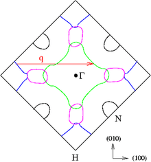
Some solids with a high form density waves while others choose a superconducting or magnetic ground state at low temperatures, because of the existence of nesting vectors in the materials' Fermi surfaces. The concept of a nesting vector is illustrated in the Figure for the famous case of chromium, which transitions from a paramagnetic to SDW state at a Néel temperature of 311 K. Cr is a body-centered cubic metal whose Fermi surface features many parallel boundaries between electron pockets centered at and hole pockets at H. These large parallel regions can be spanned by the nesting wavevector shown in red. The real-space periodicity of the resulting spin-density wave is given by . The formation of an SDW with a corresponding spatial frequency causes the opening of an energy gap that lowers the system's energy. The existence of the SDW in Cr was first posited in 1960 by Albert Overhauser of Purdue. The theory of CDWs was first put forth by Rudolf Peierls of Oxford University, who was trying to explain superconductivity.
Many low-dimensional solids have anisotropic Fermi surfaces that have prominent nesting vectors. Well-known examples include layered materials like NbSe3,[1] TaSe2[2] and K0.3MoO3 (a Chevrel phase)[3] and quasi-1D organic conductors like TMTSF or TTF-TCNQ.[4] CDWs are also common at the surface of solids where they are more commonly called surface reconstructions or even dimerization. Surfaces so often support CDWs because they can be described by two-dimensional Fermi surfaces like those of layered materials. Chains of Au and In on semiconducting substrates have been shown to exhibit CDWs.[5] More recently, monatomic chains of Co on a metallic substrate were experimentally shown to exhibit a CDW instability and was attributed to ferromagnetic correlations.[6]
The most intriguing properties of density waves are their dynamics. Under an appropriate electric field or magnetic field, a density wave will "slide" in the direction indicated by the field due to the electrostatic or magnetostatic force. Typically the sliding will not begin until a "depinning" threshold field is exceeded where the wave can escape from a potential well caused by a defect. The hysteretic motion of density waves is therefore not unlike that of dislocations or magnetic domains. The current-voltage curve of a CDW solid therefore shows a very high electrical resistance up to the depinning voltage, above which it shows a nearly ohmic behavior. Under the depinning voltage (which depends on the purity of the material), the crystal is an insulator.
See also
References
- ↑ G. Grüner The dynamics of charge-density waves
- ↑ Mutka et al., Charge-density waves and localization in electron-irradiated 1T-TaS2
- ↑ Pouget et al., Neutron-scattering investigations of the Kohn anomaly and of the phase and amplitude charge-density-wave excitations of the blue bronze K0.3MoO3
- ↑ Patton Conductivity, Superconductivity, and the Peierls Instability
- ↑ Snijders, P. C.; Weitering, H. H. (2010). "Electronic instabilities in self-assembled atom wires". Rev. Mod. Phys. 82: 307–329. Bibcode:2010RvMP...82..307S. doi:10.1103/RevModPhys.82.307.
- ↑ Zaki, Nader; et al. (2013). "Experimental observation of spin-exchange-induced dimerization of an atomic one-dimensional system". Phys. Rev. B. 87: 161406(R). Bibcode:2013PhRvB..87p1406Z. doi:10.1103/PhysRevB.87.161406.
General References
- A pedagogical article about the topic: "Charge and Spin Density Waves," Stuart Brown and George Gruner, Scientific American 270, 50 (1994).
- Authoritative work on Cr: "Spin-density-wave antiferromagnetism in chromium," E. Fawcett, Rev. Mod. Phys. 60, 209 (1988).
- About Fermi surfaces and nesting: Electronic Structure and the Properties of Solids, Walter A. Harrison, ISBN 0-486-66021-4.
- Observation of CDW by ARPES: "Pseudogap and Charge Density Waves in Two Dimensions," S. V. Borisenko et al., Phys. Rev. Lett. 100, 196402 (2008).
- Peierls instability.
- An extensive review of experiments as of 2013 by Pierre Monceau. Electronic crystals: an experimental overview.