SMIF (interface)

SMIF (Standard Mechanical Interface) is an isolation technology developed in the 1980s by a group known as the "micronauts" at Hewlett-Packard in Palo Alto. The system is used in semiconductor wafer fabrication and cleanroom environments. It is a SEMI standard.[1]
Development
The core development team was led by Ulrich Kaempf as engineering manager, under the direction of Mihir Parikh. The core team that developed the technology was driven by Barclay Tullis, who held most of the patents, with Dave Thrasher, who later joined the Silicon Valley Group, and Thomas Atchison, a member of the technical staff under direction of Barclay Tullis. Mihir later provided the technology to SEMI, and then licensed a copy for himself, and spun out Asyst Technologies to provide the technology commercially.
Use
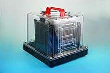
The purpose of SMIF pods is to isolate wafers from contamination by providing a miniature environment with controlled airflow, pressure and particle count. SMIF pods can be accessed by automated mechanical interfaces on production equipment. The wafers therefore remain in a carefully controlled environment whether in the SMIF pod or in a tool, without being exposed to the surrounding airflow.
Each SMIF pod contains a wafer cassette in which the wafers are stored horizontally. The bottom surface of the pod is the opening door, and when a SMIF pod is placed on a load port, the bottom door and cassette are lowered into the tool so that the wafers can be removed.
Both wafers and reticles can be handled by SMIF pods in a semiconductor fabrication environment. Used in lithographic tools, reticles or photomasks contain the image that is exposed on a coated wafer in one processing step of a complete integrated semiconductor manufacturing cycle. Because reticles are linked so directly with wafer processing, they also require steps to protect them from contamination or from being the source of contamination in the litho tool.
SMIF is typically used for wafers no larger than 200mm, the equivalent for 300mm wafers being the FOUP (Front Opening Unified Pod). The greater flexibility of 300mm wafers means that it is not feasible to use SMIF technology and designs for 300mm, hence the reason for the emergence of FOUPs. Several FOUP SEMI standards, including SEMI E47.1-1106,[2] are related to both 300 and 450 mm wafers.
See also
References
External links
- Semiconductor Equipment and Materials International - SEMI the semiconductor industry trade association
- Entegris wafer and reticle handling systems
- Fortrend Engineering