Pentium III
 | |
| Produced | From early 1999 to 2003 |
|---|---|
| Common manufacturer(s) |
|
| Max. CPU clock rate | 450 MHz to 1.4 GHz |
| FSB speeds | 100 MHz to 133 MHz |
| Min. feature size | 0.25 µm to 0.13 µm |
| Instruction set | IA-32, MMX, SSE |
| Microarchitecture | P6 |
| Cores | 1 |
| Socket(s) | |
| Predecessor | Pentium II |
| Successor | Pentium 4, Xeon, Celeron, Pentium M |
| Core name(s) |
|
The Pentium III[1] (marketed as Intel Pentium III Processor, informally PIII, also stylized as Pentium !!! ) brand refers to Intel's 32-bit x86 desktop and mobile microprocessors based on the sixth-generation P6 microarchitecture introduced on February 26, 1999. The brand's initial processors were very similar to the earlier Pentium II-branded microprocessors. The most notable differences were the addition of the SSE instruction set (to accelerate floating point and parallel calculations), and the introduction of a controversial serial number embedded in the chip during the manufacturing process.
Processor cores
Similarly to the Pentium II it superseded, the Pentium III was also accompanied by the Celeron brand for lower-end versions, and the Xeon for high-end (server and workstation) derivatives. The Pentium III was eventually superseded by the Pentium 4, but its Tualatin core also served as the basis for the Pentium M CPUs, which used many ideas from the P6 microarchitecture. Subsequently, it was the Pentium M microarchitecture of Pentium M branded CPUs, and not the NetBurst found in Pentium 4 processors, that formed the basis for Intel's energy-efficient Core microarchitecture of CPUs branded Core 2, Pentium Dual-Core, Celeron (Core), and Xeon.
| Intel Pentium III processor family | ||||
|---|---|---|---|---|
| Standard Logo (1999-2002) | Mobile Logo (1999-2003) | Desktop | ||
| Code-named | Core | Date released | ||
 |
 |
Katmai Coppermine Coppermine T Tualatin |
(250 nm) (180 nm) (180 nm) (130 nm) |
May 1999 Mar 2000 Aug 2000 Apr 2001 |
| List of Intel Pentium III microprocessors | ||||
Katmai

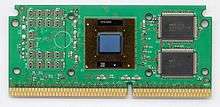
The first Pentium III variant was the Katmai (Intel product code 80525). It was a further development of the Deschutes Pentium II. The Pentium III saw an increase of 2 million transistors over the Pentium II. The differences were the addition of execution units and SSE instruction support, and an improved L1 cache controller (the L2 cache controller was left unchanged, as it would be completely redesigned for Coppermine anyway), which were responsible for the minor performance improvements over the "Deschutes" Pentium IIs. It was first released at speeds of 450 and 500 MHz in February 1999. Two more versions were released: 550 MHz on May 17, 1999 and 600 MHz on August 2, 1999. On September 27, 1999 Intel released the 533B and 600B running at 533 & 600 MHz respectively. The 'B' suffix indicated that it featured a 133 MHz FSB, instead of the 100 MHz FSB of previous models.
The Katmai contains 9.5 million transistors, not including the 512 Kbytes L2 cache (which adds 25 million transistors), and has dimensions of 12.3 mm by 10.4 mm (128 mm2). It is fabricated in Intel's P856.5 process, a 0.25 micrometre CMOS process with five levels of aluminum interconnect.[2] The Katmai used the same slot-based design as the Pentium II but with the newer SECC2 cartridge that allowed direct CPU core contact with the heat sink. There have been some early models of the Pentium III with 450 and 500 MHz packaged in an older SECC cartridge intended for OEMs.
A notable stepping for enthusiasts was SL35D. This version of Katmai was officially rated for 450 MHz, but often contained cache chips for the 600 MHz model and thus usually was capable of running at 600 MHz.
Coppermine

The second version, codenamed Coppermine (Intel product code: 80526), was released on October 25, 1999, running at 500, 533, 550, 600, 650, 667, 700, and 733 MHz. From December 1999 to May 2000, Intel released Pentium IIIs running at speeds of 750, 800, 850, 866, 900, 933 and 1000 MHz (1 GHz). Both 100 MHz FSB and 133 MHz FSB models were made. An "E" was appended to the model name to indicate cores using the new 0.18 μm fabrication process. An additional "B" was later appended to designate 133 MHz FSB models, resulting in an "EB" suffix. In terms of overall performance, the Coppermine held a slight advantage over the AMD Athlons it was released against, which was reversed when AMD applied their own die shrink and added an on-die L2 cache to the Athlon. Athlon held the advantage in floating-point intensive code, while the Coppermine could perform better when SSE optimizations were used, but in practical terms there was little difference in how the two chips performed, clock-for-clock. However, AMD were able to clock the Athlon higher, reaching speeds of 1.2 GHz before the launch of the Pentium 4.
A 1.13 GHz version was released in mid-2000 but famously recalled after a collaboration between HardOCP and Tom's Hardware[3] discovered various instabilities with the operation of the new CPU speed grade. The Coppermine core was unable to reliably reach the 1.13 GHz speed without various tweaks to the processor's microcode, effective cooling, additional voltage (1.75 V vs. 1.65 V), and specifically validated platforms.[4] Intel only officially supported the processor on its own VC820 i820-based motherboard, but even this motherboard displayed instability in the independent tests of the hardware review sites. In benchmarks that were stable, performance was shown to be sub-par, with the 1.13 GHz CPU equalling a 1.0 GHz model. Tom's Hardware attributed this performance deficit to relaxed tuning of the CPU and motherboard to improve stability.[5] Intel needed at least six months to resolve the problems using a new cD0 stepping and re-released 1.1 GHz and 1.13 GHz versions in 2001.
Microsoft's Xbox game console uses a variant of the Pentium III/Mobile Celeron family in a Micro-PGA2 form factor. The sSpec designator of the chips is SL5Sx, which makes it most similar to the Mobile Celeron Coppermine-128 processor. It shares with the Coppermine-128 Celeron its 128 KB L2 cache, and 180 nm process technology.[6]
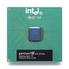
Major improvements introduced with the Coppermine were an on-chip L2 cache (which Intel called an Advanced Transfer Cache, or ATC) and better pipelining. The ATC operates at the core clock rate and has a capacity of 256 KB. It is eight-way set-associative and is accessed via a 256-bit bus. These features resulted in a cache with a lower latency relative to Katmai, improving performance significantly. Under competitive pressure from the AMD Athlon, Intel re-worked the internals, finally removing some well-known pipeline stalls. The result was that applications affected by these pipeline stalls ran faster on the Coppermine by up to 30%. The Coppermine contained 29 million transistors and was fabricated in a 0.18 µm process. Although its codename gives the impression that it used copper interconnects, its interconnects were in fact aluminium. The Coppermine was packaged in a 370-pin FC-PGA for use with Socket 370, or in SECC2 for Slot 1. Early versions have an exposed die, whereas later versions have an integrated heat spreader (IHS) to improve contact between the die and the heatsink. This in itself did not improve thermal conductivity, since it added another layer of metal and thermal paste between the die and the heatsink, but it greatly assisted in holding the heatsink flat against the die. Earlier Coppermines without the IHS made heatsink mounting challenging.[7] If the heatsink was not flat against the die, heat transfer efficiency was greatly reduced. Some heatsink manufacturers began providing pads on their products, similar to what AMD did with the "Thunderbird" Athlon to ensure that the heatsink was mounted flatly. The enthusiast community went so far as to create shims to assist in maintaining a flat interface.[8]
Coppermine T
This revision is an intermediate step between Coppermine and Tualatin, with support for lower-voltage system logic present on the latter but core power within previously defined voltage specs of the former so it could work in older system boards.
Intel used the latest Coppermines with the cD0-Stepping and modified them so that they worked with low voltage system bus operation at 1.25 V AGTL as well as normal 1.5 V AGTL+ signal levels, and would auto detect differential or single-ended clocking. This modification made them compatible to the latest generation Socket-370 boards supporting FC-PGA2 packaged CPUs while maintaining compatibility with the older FC-PGA boards. The Coppermine T also had two way symmetrical multiprocessing capabilities, but only in FC-PGA2 boards.
They can be distinguished from Tualatin processors by their part numbers, which include the digits: 80533 e.g. the 1133 MHz SL5QK P/N is: RK80533PZ006256, while the 1000 MHz SL5QJ P/N is: RK80533PZ001256.[9]
Tualatin

The third revision, Tualatin (80530), was a trial for Intel's new 0.13 µm process. Tualatin-based Pentium IIIs were released during 2001 until early 2002 at speeds of 1.0, 1.13, 1.2, 1.26, 1.33 and 1.4 GHz. Tualatin performed quite well, especially in variations which had 512 KB L2 cache (called the Pentium III-S). The Pentium III-S variant was mainly intended for servers, especially those where power consumption mattered, i.e., thin blade servers.
The Tualatin also formed the basis for the highly popular Pentium III-M mobile processor, which became Intel's front-line mobile chip (the Pentium 4 drew significantly more power, and so was not well-suited for this role) for the next two years. The chip offered a good balance between power consumption and performance, thus finding a place in both performance notebooks and the "thin and light" category.
The Tualatin-based Pentium III had shown superior performance compared to the fastest Willamette-based Pentium 4, and even the Thunderbird-based Athlons. In spite of this, it appears that Intel wanted to end the Pentium III's life, as they modified the Tualatin-based Pentium IIIs to be incompatible with the then-existing Socket 370 motherboards and kept the L2 cache in non-Pentium III-S models 256 KB.[10] Moreover, Intel's only officially supported chipset for Tualatins (except 3rd party server-line chipsets found on expensive server boards), the i815T, could only handle 512 MB RAM and had inferior performance because of a fixed command queue depth of 1, compared to 8 with the older BX chipset. However, the enthusiast community found a way to run Tualatins on then-ubiquitous BX chipset based boards, although it was often a non-trivial task and required some degree of technical skills.
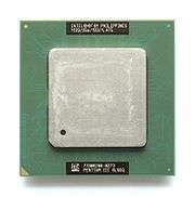
Tualatin-based Pentium III CPUs can usually be visually distinguished from Coppermine-based processors by the metal integrated heat-spreader (IHS) fixed on top of the package. However, the very last models of Coppermine Pentium IIIs also featured the IHS — the integrated heat spreader is actually what distinguishes the FC-PGA2 package from the FC-PGA — both are for Socket 370 motherboards.[11]
Before the addition of the heat spreader, it was sometimes difficult to install a heatsink on a Pentium III. One had to be careful not to put force on the core at an angle because doing so would cause the edges and corners of the core to crack and could destroy the CPU. It was also sometimes difficult to achieve a flat mating of the CPU and heatsink surfaces, a factor of critical importance to good heat transfer. This became increasingly challenging with the socket 370 CPUs, compared with their Slot 1 predecessors, because of the force required to mount a socket-based cooler and the narrower, 2-sided mounting mechanism (Slot 1 featured 4-point mounting). As such, and because the 0.13 µm Tualatin had an even smaller core surface area than the 0.18 µm Coppermine, Intel installed the metal heatspreader on Tualatin and all future desktop processors.
The Tualatin core was named after the Tualatin Valley and Tualatin River in Oregon, where Intel has large manufacturing and design facilities.
Pentium III's SSE implementation

Since Katmai was built in the same 0.25 µm process as Pentium II "Deschutes", it had to implement SSE using as little silicon as possible. To achieve this goal, Intel implemented the 128-bit architecture by double-cycling the existing 64-bit data paths and by merging the SIMD-FP multiplier unit with the x87 scalar FPU multiplier into a single unit. To utilize the existing 64-bit data paths, Katmai issues each SIMD-FP instruction as two μops. To compensate partially for implementing only half of SSE’s architectural width, Katmai implements the SIMD-FP adder as a separate unit on the second dispatch port. This organization allows one half of a SIMD multiply and one half of an independent SIMD add to be issued together bringing the peak throughput back to four floating point operations per cycle — at least for code with an even distribution of multiplies and adds.[12]
The issue was that Katmai’s hardware-implementation contradicted the parallelism model implied by the SSE instruction-set. Programmers faced a code-scheduling dilemma: Should the SSE-code be tuned for Katmai's limited execution resources, or should it be tuned for a future processor with more resources? Katmai-specific SSE optimizations yielded the best possible performance from the Pentium III family but was suboptimal for later Intel processors, such as the Pentium 4 and Core.
Core specifications
Katmai (0.25 µm)
- L1-Cache: 16 + 16 KB (data + instructions)
- L2-Cache: 512 KB, external chips on CPU module at 50% of CPU-speed
- MMX, SSE
- Slot 1 (SECC, SECC2)
- VCore: 2.0 V, (600 MHz: 2.05 V)
- Clockrate: 450–600 MHz
- 100 MHz FSB: 450, 500, 550, 600 MHz (These models have no letter after the speed)
- 133 MHz FSB: 533, 600 MHz
Coppermine (0.18 µm)
- L1-Cache: 16 + 16 KB (data + instructions)
- L2-Cache: 256 KB, fullspeed
- MMX, SSE
- Slot 1 (SECC2), Socket 370 (FC-PGA)
- Front side bus: 100, 133 MHz
- VCore: 1.6 V, 1.65 V, 1.70 V, 1.75 V
- First release: October 25, 1999
- Clockrate: 500–1133 MHz
- 100 MHz FSB: 500, 550, 600, 650, 700, 750, 800, 850, 900, 1000, 1100 MHz (E-Models)
- 133 MHz FSB: 533, 600, 667, 733, 800, 866, 933, 1000, 1133 MHz (EB-Models)
Coppermine T (0.18 µm)
- L1-Cache: 16 + 16 KB (data + instructions)
- L2-Cache: 256 KB, fullspeed
- MMX, SSE
- Socket 370 (FC-PGA, FC-PGA2)
- Front side bus: 133 MHz
- VCore: 1.75 V
- First release: August 2000
- Clockrate: 800–1133 MHz
- 133 MHz FSB: 800, 866, 933, 1000, 1133 MHz
Tualatin (0.13 µm)
- L1-Cache: 16 + 16 KB (data + instructions)
- L2-Cache: 256 or 512 KB, fullspeed
- MMX, SSE, Hardware prefetch
- Socket 370 (FC-PGA2)
- Front side bus: 133 MHz
- VCore: 1.45, 1.475 V
- First release: 2001
- Clockrate: 1000–1400 MHz
- Pentium III (256 KB L2-Cache): 1000, 1133, 1200, 1333, 1400 MHz
- Pentium III-S (512 KB L2-Cache): 1133, 1266, 1400 MHz
Controversy about privacy issues
The Pentium III was the first x86 CPU to include a unique, retrievable, identification number, called PSN (Processor Serial Number). A Pentium III's PSN can be read by software through the CPUID instruction if this feature has not been disabled through the BIOS.
On November 29, 1999, the Science and Technology Options Assessment (STOA) Panel of the European Parliament, following their report on electronic surveillance techniques asked parliamentary committee members to consider legal measures that would "prevent these chips from being installed in the computers of European citizens."[13]
Intel eventually removed the PSN feature from Tualatin-based Pentium IIIs, and the feature was not present in Pentium 4 or Pentium M.
See also
- Intel Pentium 4 microprocessor
- List of Intel Pentium III microprocessors
- List of Intel Celeron microprocessors
References
- ↑ Microprocessor Hall of Fame, Intel Corporation, archived from the original on April 6, 2008, retrieved August 11, 2007
- ↑ Diefendorff, Keith (March 8, 1999). "Pentium III = Pentium II + SSE". Microprocessor Report.
- ↑ Pabst, Thomas. "Intel Admits Problems With Pentium III 1.13 GHz: Production and Shipments Halted". Tom's Hardware.
- ↑ Pabst, Thomas. Intel Admits Problems With Pentium III 1.13 GHz: Production and Shipments Halted, Tom's Hardware, August 28, 2000.
- ↑ Pabst, Thomas. Latest Update On Intel's 1.13 GHz Pentium III, Tom's Hardware, August 28, 2000.
- ↑ VHJ: More on the Xbox CPU
- ↑ Alpha FC-PAL35T & POP66T Cooler Review, The Tech Zone, April 12, 2000.
- ↑ Verbist, Tim. Copper Shims, Overclockers Online, December 3, 2000.
- ↑ Intel Pentium III Coppermine-T core, retrieved July 8, 2010
- ↑ http://www.emulators.com/docs/pentium_3.htm
- ↑ Lal Shimpi, Anand. Intel Pentium III 1.2 GHz 0.13-micron Tualatin: The Celeron of the Future, Anandtech, July 30, 2001.
- ↑ Diefendorff, Keith (March 8, 1999). "Pentium III = Pentium II + SSE: Internet SSE Architecture Boosts Multimedia Performance". Microprocessor Report. Volume 13, Number 3.
- ↑ Advisory group asks EU to consider Pentium III ban, CNN, November 29, 1999.
External links
- Listing of various PII, PIII, and Celeron alphanumeric model designations
- Comparison of 7th generation x86 CPU architectures
- Intel FAQ about the pentium III processor serial number