Sheet resistance

Sheet resistance is a measure of resistance of thin films that are nominally uniform in thickness. It is commonly used to characterize materials made by semiconductor doping, metal deposition, resistive paste printing, and glass coating. Examples of these processes are: doped semiconductor regions (e.g., silicon or polysilicon), and the resistors that are screen printed onto the substrates of thick-film hybrid microcircuits.
The utility of sheet resistance as opposed to resistance or resistivity is that it is directly measured using a four-terminal sensing measurement (also known as a four-point probe measurement) or indirectly by using a non-contact eddy current based testing device. Sheet resistance is invariable under scaling of the film contact and therefore can be used to compare the electrical properties of devices that are significantly different in size.
Calculations

Sheet resistance is applicable to two-dimensional systems in which thin films are considered two-dimensional entities. When the term sheet resistance is used, it is implied that the current is along the plane of the sheet, not perpendicular to it.
In a regular three-dimensional conductor, the resistance can be written as
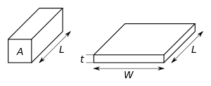
where is the resistivity, is the cross-sectional area, and is the length. The cross-sectional area can be split into the width and the sheet thickness .
Upon combining the resistivity with the thickness, the resistance can then be written as
where is the sheet resistance. If the film thickness is known, the bulk resistivity (in Ω·cm) can be calculated by multiplying the sheet resistance by the film thickness in cm:
Units
Sheet resistance is a special case of resistivity for a uniform sheet thickness. Commonly, resistivity (also known as bulk resistance, specific electrical resistance, or volume resistivity) is in units of Ω·m, which is more completely stated in units of Ω·m2/m (Ω·area/length). When divided by the sheet thickness (m), the units are Ω·m·(m/m)/m = Ω. The term "(m/m)" cancels, but represents a special "square" situation yielding an answer in ohms. An alternative, common unit is "ohms square" (denoted "") or "ohms per square" (denoted "Ω/sq" or ""), which is dimensionally equal to an ohm, but is exclusively used for sheet resistance. This is an advantage, because sheet resistance of 1 Ω could be taken out of context and misinterpreted as bulk resistance of 1 ohm, whereas sheet resistance of 1 Ω/sq cannot thus be misinterpreted.
The reason for the name "ohms per square" is that a square sheet with sheet resistance 10 ohm/square has an actual resistance of 10 ohm, regardless of the size of the square. (For a square, , so .) The unit can be thought of as, loosely, "ohms · aspect ratio". Example: A 3-unit long by 1-unit wide (aspect ratio = 3) sheet made of material having a sheet resistance of 21 Ω/sq would measure 63 Ω (since it is composed of three 1-unit by 1-unit squares), if the 1-unit edges were attached to an ohmmeter that made contact entirely over each edge.
For semiconductors
For semiconductors doped through diffusion or surface peaked ion implantation we define the sheet resistance using the average resistivity of the material:
which in materials with majority-carrier properties can be approximated by (neglecting intrinsic charge carriers):
where is the junction depth, is the majority-carrier mobility, is the carrier charge, and is the net impurity concentration in terms of depth. Knowing the background carrier concentration and the surface impurity concentration, the sheet resistance-junction depth product can be found using Irvin's curves, which are numerical solutions to the above equation.
Measurement
A four-point probe is used to avoid contact resistance, which can often have the same magnitude as the sheet resistance. Typically a constant current is applied to two probes, and the potential on the other two probes is measured with a high-impedance voltmeter. A geometry factor needs to be applied according to the shape of the four-point array. Two common arrays are square and in-line. For more details see Van der Pauw method.
Measurement may also be made by applying high-conductivity bus bars to opposite edges of a square (or rectangular) sample. Resistance across a square area will be measured in Ω/sq. For a rectangle an appropriate geometric factor is added. Bus bars must make ohmic contact.
Inductive measurement is used as well. This method measures the shielding effect created by eddy currents. In one version of this technique a conductive sheet under test is placed between two coils. This non-contact sheet resistance measurement method also allows to characterize encapsulated thin-films or films with rough surfaces.[1]
A very crude two-point probe method is to measure resistance with the probes close together and the resistance with the probes far apart. The difference between these two resistances will be of the order of magnitude of the sheet resistance.
Typical applications
Sheet resistance measurements are very common to characterize the uniformity of conductive or semiconductive coatings and materials, e.g. for quality assurance. Typical applications include the inline process control of metal, TCO, conductive nanomaterials or other coatings on architectural glass, wafers, flat panel displays, polymer foils, OLED, ceramics, etc. The contacting four-point probe is often applied for single-point measurements of hard or coarse materials. Non-contact eddy current systems are applied for sensitive or encapsulated coatings, for inline measurements and for high-resolution mapping.
See also
References
- ↑ Overview on non-contact eddy current sheet resistance measurement techniques and benefits, retrieved 22 November 2013.
General references
- Van Zant, Peter (2000). Microchip Fabrication. New York: McGraw-Hill. pp. 431–2. ISBN 0-07-135636-3.
- Jaeger, Richard C. (2002). Introduction to Microelectronic Fabrication (2nd ed.). New Jersey: Prentice Hall. pp. 81–88. ISBN 0-201-44494-1.
- Schroder, Dieter K. (1998). Semiconductor Material and Device Characterization. New York: J Wiley & Sons. pp. 1–55. ISBN 0-471-24139-3.