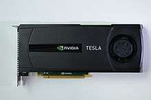
Nvidia Tesla
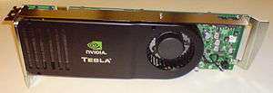 |
Nvidia Tesla is Nvidia's brand name for their products targeting stream processing and/or general purpose GPU. Products use GPUs from the G80 series onward. The underlying Tesla microarchitecture of the GPUs and the Tesla product line are named after pioneering electrical engineer Nikola Tesla.
Overview
With their very high computational power (measured in floating point operations per second or FLOPS) compared to microprocessors, the Tesla products target the high-performance computing market.[1] As of 2012, Nvidia Teslas power some of the world's fastest supercomputers, including Titan at Oak Ridge National Laboratory and Tianhe-1A, in Tianjin, China.
The lack of ability to output images to a display was the main difference between Tesla products and the consumer level GeForce cards and the professional level Nvidia Quadro cards, but the latest Tesla C-class products include one Dual-Link DVI port.[2] For equivalent single precision output, Fermi-based Nvidia GeForce cards have four times less dual-precision performance. Tesla products primarily operate:[3]
- in simulations and in large scale calculations (especially floating-point calculations)
- for high-end image generation for applications in professional and scientific fields
- with the use of OpenCL or CUDA.
Nvidia intends to offer ARMv8 processor cores embedded into future Tesla GPUs as part of Project Denver.[4] This will be a 64-bit follow on to the 32-bit Tegra chips.
Market
The defense industry currently accounts for less than a sixth of Tesla sales, but Sumit Gupta predicts further sales to the geospatial intelligence market.[5]
Specifications and configurations
- 1 Specifications not specified by Nvidia assumed to be based on the GeForce 8800GTX
- 2 Specifications not specified by Nvidia assumed to be based on the GeForce GTX 280
- 3 Specifications not specified by Nvidia are assumed to be based on the GeForce 400 series
- 4 With ECC on, a portion of the dedicated memory is used for ECC bits, so the available user memory is reduced by 12.5%. (e.g. 4 GB total memory yields 3.5 GB of user available memory.)
- 5 To calculate the processing power see Tesla (microarchitecture)#Performance, Fermi (microarchitecture)#Performance, Kepler (microarchitecture)#Performance, Maxwell (microarchitecture)#Performance, or Pascal (microarchitecture)#Performance. A number range specifies the minimum and maximum processing power at, respectively, the base clock and maximum boost clock.
- 6 Specifications not specified by Nvidia assumed to be based on the Quadro FX 5800
- 7 GPU Boost is a default feature that increases the core clock rate while remaining under the card's predetermined power budget. Multiple boost clocks are available, but this table lists the highest clock supported by each card.[6]
- 8 Core architecture version according to the CUDA programming guide.
- For the basic specifications of Tesla, refer to the GPU Computing Processor specifications.
- Because of Tesla's non-output nature, fillrate and graphics API compatibility are not applicable.
| Model | Micro- architecture |
Launch | Chips | Core clock (MHz) |
Shaders | Memory | Processing power (GFLOPS)5 | CUDA compute ability8 |
TDP (Watts) |
Notes, form_factor | ||||||||
|---|---|---|---|---|---|---|---|---|---|---|---|---|---|---|---|---|---|---|
| Cuda cores (total) |
Base clock (MHz) | Max Boost Clock (MHz)7 |
Bus type | Bus width (bit) |
Size (GB) |
Clock (MT/s) |
Bandwidth (GB/s) |
Single precision (MAD+MUL) |
Single precision (MAD or FMA) |
Double precision (FMA) | ||||||||
| Units | MHz | MHz | W | |||||||||||||||
| C870 GPU Computing Module1 | Tesla | 1× G80 | 600 | 128 | 1350 | N/A | GDDR3 | 384 | 1.5 | 1600 | 76.8 | 518.4 | 345.6 | No | 1.0 | 170.9 | Internal PCIe GPU (full-height, dual-slot) | |
| D870 Deskside Computer1 | 2× G80 | 600 | 256 | 1350 | N/A | GDDR3 | 2× 384 | 2× 1.5 | 1600 | 2× 76.8 | 1036.8 | 691.2 | No | 1.0 | 520 | Deskside or 3U rack-mount external GPUs | ||
| S870 GPU Computing Server1 | 4× G80 | 600 | 512 | 1350 | N/A | GDDR3 | 4× 384 | 4× 1.5 | 1600 | 4× 76.8 | 2073.6 | 1382.4 | No | 1.0 | 1U rack-mount external GPUs, connect via 2× PCIe (×16) | |||
| C1060 GPU Computing Module2 | 1× GT200 | 602 | 240 | 1296[7] | N/A | GDDR3 | 512 | 4 | 1600 | 102.4 | 933.12 | 622.08 | 77.76 | 1.3 | 187.8 | Internal PCIe GPU (full-height, dual-slot) | ||
| S1070 GPU Computing Server "400 configuration"2 | 4× GT200 | 602 | 960 | 1296 | N/A | GDDR3 | 4× 512 | 4× 4 | 1538.4 | 4× 98.5 | 3732.5 | 2488.3 | 311.0 | 1.3 | 800 | 1U rack-mount external GPUs, connect via 2× PCIe (×8 or ×16) | ||
| S1070 GPU Computing Server "500 configuration"2 | 1440 | N/A | 4147.2 | 2764.8 | 345.6 | |||||||||||||
| S1075 GPU Computing Server2[8] | 4× GT200 | 602 | 960 | 1440 | N/A | GDDR3 | 4× 512 | 4× 4 | 1538.4 | 4× 98.5 | 4147.2 | 2764.8 | 345.6 | 1.3 | 1U rack-mount external GPUs, connect via 1× PCIe (×8 or ×16) | |||
| Quadro Plex 2200 D2 Visual Computing System6 | 2× GT200GL | 648 | 480 | 1296 | N/A | GDDR3 | 2× 512 | 2× 4 | 1600 | 2× 102.4 | 1866.2 | 1244.2 | 155.5 | 1.3 | Deskside or 3U rack-mount external GPUs with 4 dual-link DVI outputs | |||
| Quadro Plex 2200 S4 Visual Computing System6 | 4× GT200GL | 648 | 960 | 1296 | N/A | GDDR3 | 4× 512 | 4× 4 | 1600 | 4× 102.4 | 3732.5 | 2488.3 | 311.0 | 1.3 | 1200 | 1U rack-mount external GPUs, connect via 2× PCIe (×8 or ×16) | ||
| C2050 GPU Computing Module[9] | Fermi | 1× GF100 | 575 | 448 | 1150 | N/A | GDDR5 | 384 | 34 | 3000 | 144 | No | 1030.4 | 515.2 | 2.0 | 247 | Internal PCIe GPU (full-height, dual-slot) | |
| M2050 GPU Computing Module[10] | N/A | 3092 | 148.4 | No | 225 | |||||||||||||
| C2070 GPU Computing Module[9] | 1× GF100 | 575 | 448 | 1150 | N/A | GDDR5 | 384 | 64 | 3000 | 144 | No | 1030.4 | 515.2 | 2.0 | 247 | Internal PCIe GPU (full-height, dual-slot) | ||
| C2075 GPU Computing Module[11] | N/A | 3000 | 144 | No | 225 | |||||||||||||
| M2070/M2070Q GPU Computing Module[12] | N/A | 3132 | 150.336 | No | 225 | |||||||||||||
| M2090 GPU Computing Module[13] | 1× GF110 | 650 | 512 | 1300 | N/A | GDDR5 | 384 | 64 | 3700 | 177.6 | No | 1331.2 | 665.6 | 2.0 | 225 | Internal PCIe GPU (full-height, dual-slot) | ||
| S2050 GPU Computing Server | 4× GF100 | 575 | 1792 | 1150 | N/A | GDDR5 | 4× 384 | 4× 34 | 3 | 4× 148.4 | No | 4121.6 | 2060.8 | 2.0 | 900 | 1U rack-mount external GPUs, connect via 2× PCIe (×8 or ×16) | ||
| S2070 GPU Computing Server | N/A | 4× 64 | No | |||||||||||||||
| K10 GPU Accelerator[14] | Kepler | May 1, 2012 | 2× GK104 | N/A | 3072 | 745 | ? | GDDR5 | 2× 256 | 2× 4 | 5000 | 2× 160 | No | 4577 | 190.7 | 3.0 | 225 | Internal PCIe GPU (full-height, dual-slot) |
| K20 GPU Accelerator[15][16] | November 12, 2012 | 1× GK110 | N/A | 2496 | 706 | ? | GDDR5 | 320 | 5 | 5200 | 208 | No | 3524 | 1175 | 3.5 | 225 | Internal PCIe GPU (full-height, dual-slot) | |
| K20X GPU Accelerator[17] | 1× GK110 | N/A | 2688 | 732 | ? | GDDR5 | 384 | 6 | 5200 | 250 | No | 3935 | 1312 | 3.5 | 235 | Internal PCIe GPU (full-height, dual-slot) | ||
| K40 GPU Accelerator[18] | 1× GK110B | N/A | 2880 | 745 | 875 | GDDR5 | 384 | 124 | 6000 | 288 | No | 4291–5040 | 1430–1680 | 3.5 | 235 | Internal PCIe GPU (full-height, dual-slot) | ||
| K80 GPU Accelerator[19] | November 17, 2014 | 2× GK210 | N/A | 4992 | 560 | 875 | GDDR5 | 2× 384 | 2× 12 | 5000 | 2× 240 | No | 5591–8736 | 1864–2912 | 3.7 | 300 | Internal PCIe GPU (full-height, dual-slot) | |
| M4 GPU Accelerator[20][21] | Maxwell | 1× GM206 | N/A | 1024 | 872 | 1072 | GDDR5 | 128 | 4 | 5500 | 88 | No | 1786–2195 | 55.81–68.61 | 5.2 | 50–75 | Internal PCIe GPU (half-height, single-slot) | |
| M6 GPU Accelerator[22] | 1× GM204 | N/A | 1536 | 722 | 1051 | GDDR5 | 256 | 8 | 4600 | 147.2 | No | 2218–3229 | 69.3–100.9 | 5.2 | 75–100 | Internal MXM GPU | ||
| M10 GPU Accelerator[23] | 4× GM107 | N/A | 2560 | 1033 | ? | GDDR5 | 4× 128 | 4× 8 | 5188 | 4× 83 | No | 5289 | 165.3 | 5.2 | 225 | Internal PCIe GPU (full-height, dual-slot) | ||
| M40 GPU Accelerator[21][24] | 1× GM200 | N/A | 3072 | 948 | 1114 | GDDR5 | 384 | 12 | 6000 | 288 | No | 5825–6844 | 182.0–213.9 | 5.2 | 250 | Internal PCIe GPU (full-height, dual-slot) | ||
| M60 GPU Accelerator[25] | August 30, 2015 | 2× GM204 | N/A | 4096 | 899 | 1178 | GDDR5 | 2× 256 | 2× 8 | 5000 | 2× 160 | No | 7365–9650 | 230.1–301.6 | 5.2 | 225–300 | Internal PCIe GPU (full-height, dual-slot) | |
| P4 GPU Accelerator[26] | Pascal | September 13, 2016 | 1× GP104 | N/A | 2560 | 810 | 1063 | GDDR5 | 256 | 8 | 6000 | 192.0 | No | 4147–5443 | 129.6–170.1 | 6.1 | 50-75 | PCIe card |
| P40 GPU Accelerator[26] | September 13, 2016 | 1× GP102 | N/A | 3840 | 1303 | 1531 | GDDR5 | 384 | 24 | 7200 | 345.6 | No | 10007–11758 | 312.7–367.4 | 6.1 | 250 | PCIe card | |
| P100 GPU Accelerator (Mezzanine)[27][28] | 1× GP100 | N/A | 3584 | 1328 | 1480 | HBM2 | 4096 | 16 | 1406 | 720 | No | 9519–10609 | 4760–5304 | 6.0 | 300 | NVLink card | ||
| P100 GPU Accelerator (16 GB Card)[29] | June 20, 2016 | N/A | 1126 | 1303 | No | 8071‒9340 | 4036‒4670 | 250 | PCIe card | |||||||||
| P100 GPU Accelerator (12 GB Card)[29] | N/A | 3072 | 12 | 540 | No | 8071‒9340 | 4036‒4670 | |||||||||||
| V100 GPU Accelerator (Mezzanine )[30][31][32] | Volta | 1× GV100 | N/A | 5120 | Unknown | 1455 | HBM2 | 4096 | 16 | 1750 | 900 | No | 14899 | 7450 | 7.0 | 300 | NVlink Card | |
| V100 GPU Accelerator (PCIe card)[30][31][32] | May 10, 2017 | N/A | Unknown | 1370 | No | 14028 | 7014 | 250 | PCIe card | |||||||||
| Model | Micro- architecture |
Launch | Chips | Core clock (MHz) |
Shaders | Memory | Processing power (GFLOPS)5 | CUDA compute ability |
TDP (Watts) |
Notes, form factor | ||||||||
| Cuda cores (total) |
Base clock (MHz) | Max Boost Clock (MHz)7 |
Bus type | Bus width (bit) |
Size (GB) |
Clock (MT/s) |
Bandwidth (total) (GB/s) |
Single precision (MAD+MUL) |
Single precision (MAD or FMA) |
Double precision (FMA) | ||||||||
See also
References
- ↑ High Performance Computing - Supercomputing with Tesla GPUs
- ↑
- ↑ Tesla Technical Brief (PDF)
- ↑ "Nvidia to Integrate ARM Processors in Tesla." (Article from 2012)
- ↑ "Nvidia chases defense, intelligence ISVs with GPUs."
- ↑ "Nvidia GPU Boost For Tesla" (PDF). January 2014. Retrieved 7 December 2015.
- ↑ "Tesla C1060 Computing Processor Board" (PDF). Nvidia.com. Retrieved 2015-12-11.
- ↑ "Difference between Tesla S1070 and S1075". 31 October 2008. Retrieved January 29, 2017.
S1075 has one interface card
- 1 2 "Tesla C2050 and Tesla C2070 Computing Processor" (PDF). Nvidia.com. Retrieved 2015-12-11.
- ↑ "Tesla M2050 and Tesla M2070/M2070Q Dual-Slot Computing Processor Modules" (PDF). Nvidia.com. Retrieved 2015-12-11.
- ↑ "Tesla C2075 Computing Processor Board" (PDF). Nvidia.com. Retrieved 2015-12-11.
- ↑ Hand, Randall (2010-08-23). "NVidia Tesla M2050 & M2070/M2070Q Specs OnlineVizWorld.com". VizWorld.com. Retrieved 2015-12-11.
- ↑ "Tesla M2090 Dual-Slot Computing Processor Module" (PDF). Nvidia.com. Retrieved 2015-12-11.
- ↑ "Tesla K10 GPU Accelerator" (PDF). Nvidia.com. Retrieved 2015-12-11.
- ↑ "Tesla K20 GPU Active accelerator" (PDF). Nvidia.com. Retrieved 2015-12-11.
- ↑ "Tesla K20 GPU Accelerator" (PDF). Nvidia.com. Retrieved 2015-12-11.
- ↑ "Tesla K20X GPU Accelerator" (PDF). Nvidia.com. Retrieved 2015-12-11.
- ↑ "Tesla K40 GPU Accelerator" (PDF). Nvidia.com. Retrieved 2015-12-11.
- ↑ "Tesla K80 GPU Accelerator" (PDF). Images.nvidia.com. Retrieved 2015-12-11.
- ↑ "Nvidia Announces Tesla M40 & M4 Server Cards - Data Center Machine Learning". Anandtech.com. Retrieved 2015-12-11.
- 1 2 "Accelerating Hyperscale Datacenter Applications with Tesla GPUs | Parallel Forall". Devblogs.nvidia.com. 2015-11-10. Retrieved 2015-12-11.
- ↑ "Tesla M6" (PDF). Images.nvidia.com. Retrieved 2016-05-28.
- ↑ "Tesla M10" (PDF). Images.nvidia.com. Retrieved 2016-10-29.
- ↑ "Tesla M40" (PDF). Images.nvidia.com. Retrieved 2015-12-11.
- ↑ "Tesla M60" (PDF). Images.nvidia.com. Retrieved 2016-05-27.
- 1 2 Smith, Ryan (13 September 2016). "Nvidia Announces Tesla P40 & Tesla P4 - Network Inference, Big & Small". Anandtech. Retrieved 13 September 2016.
- ↑ Smith, Ryan (5 April 2016). "Nvidia Announces Tesla P100 Accelerator - Pascal GP100 for HPC". Anandtech.com. Anandtech.com. Retrieved 5 April 2016.
- ↑ Harris, Mark. "Inside Pascal: Nvidia’s Newest Computing Platform". Retrieved 13 September 2016.
- 1 2 Smith, Ryan (20 June 2016). "NVidia Announces PCI Express Tesla P100". Anandtech.com. Retrieved 21 June 2016.
- 1 2 Smith, Ryan (10 May 2017). "The Nvidia GPU Technology Conference 2017 Keynote Live Blog". Anandtech. Retrieved 10 May 2017.
- 1 2 Smith, Ryan (10 May 2017). "NVIDIA Volta Unveiled: GV100 GPU and Tesla V100 Accelerator Announced". Anandtech. Retrieved 10 May 2017.
- 1 2 Oh, Nate (20 June 2017). "NVIDIA Formally Announces V100: Available later this Year". Anandtech.com. Retrieved 20 June 2017.
External links
| Wikimedia Commons has media related to Nvidia Tesla series. |
- NVIDIA Product Overview and Technical Brief
- NVIDIA's Tesla homepage
- Nvidia Tesla C2050/ C2070 GPU Computing Processor
- Nvidia Tesla S2050 GPU Computing System
- Nvidia Tesla C1060 Computing Processor
- Nvidia Tesla S1070
- Nvidia Tesla M1060 Processor
- Nvidia Nsight