Metal gate
A metal gate, in the context of a lateral Metal-Oxide-Semiconductor MOS stack, is just that—the gate material is made from a metal.
For decades (i.e., in the late 1970s), the industry had moved away from metal (most typically aluminum, evaporated in a vacuum chamber onto the wafer surface), as the gate material in the MOS stack due to fabrication complications. A material called polysilicon (polycrystalline silicon, highly doped with donors or acceptors to reduce its electrical resistance) was used to replace aluminum because:
- Polysilicon can be deposited easily via chemical vapor deposition (CVD) and is tolerant to subsequent manufacturing steps which involve extremely high temperatures (in excess of 900-1000 °C), where metal was not.
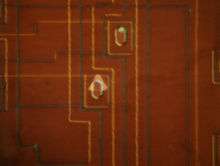
 Figure 1. Example of visual evidence of aluminum alloying into < 1 1 1 > silicon due to excessive aluminum annealing. The integrated circuit aluminum layer was removed via chemical etching to reveal this detail.
 - Particularly, metal (most commonly aluminum - a Type III (P-type) dopant) has a tendency to disperse into (alloy with) silicon during these thermal annealing steps. In particular, when used on a silicon wafer with a < 1 1 1 > crystal orientation, excessive alloying of aluminum (from extended high temperature processing steps) with the underlying silicon can create a short circuit between the diffused FET source or drain areas under the aluminum and across the metallurgical junction into the underlying substrate - causing irreparable circuit failures. These shorts are created by pyramidal-shaped spikes of silicon-aluminum alloy - pointing vertically "down" into the silicon wafer. The practical high-temperature limit for annealing aluminum on silicon is on the order of 450 °C.
- Polysilicon is also attractive for the easy manufacturing of self-aligned gates. The implantation or diffusion of source and drain dopant impurities is carried out with the gate in place, leading to a channel perfectly aligned to the gate without additional lithographic steps with the potential for misalignment of the layers.
- In NMOS and CMOS technologies, over time and elevated temperatures, the positive voltages employed by the gate structure can cause any existing positively charged sodium impurities directly under the positively charged gate to diffuse through the gate dielectric and migrate to the less-positively-charged channel surface, where the positive sodium charge has a higher effect on the channel creation - thus lowering the threshold voltage of an N-channel transistor and potentially causing failures over time. Earlier PMOS technologies were not sensitive to this effect because the positively charged sodium was naturally attracted towards the negatively charged gate, and away from the channel, minimizing threshold voltage shifts. N-channel, metal gate processes (in the 1970s) imposed a very high standard of cleanliness (absence of sodium) - difficult to achieve in that timeframe, resulting in high manufacturing costs. Polysilicon gates - while sensitive to the same phenomenon, could be exposed to small amounts of HCl gas during subsequent high-temperature processing (commonly called "gettering") to react with any sodium, binding with it to form NaCl and carrying it away in the gas stream, leaving an essentially sodium-free gate structure - greatly enhancing reliability.
However, polysilicon doped at practical levels does not offer the near-zero electrical resistance of metals, and is therefore not ideal for charging and discharging the gate capacitance of the transistor - resulting in slower circuitry.
From the 45 nm node onward, the metal gate technology returns, together with the use of high-dielectric (high-k) materials, pioneered by Intel developments.
The candidates for the metal gate electrode are probably, for NMOS, Ta, TaN, Nb (single metal gate) and for PMOS WN/RuO2 (the PMOS metal gate is normally composed by 2 layers of metal). Why two metal gate? Simply because thanks to this solution, we can improve the strain capacity on the channel (by the metal gate). Moreover, this enables less current perturbations (vibrations) in the gate (thanks to the disposition of electrons inside the metal).