Lambda diode

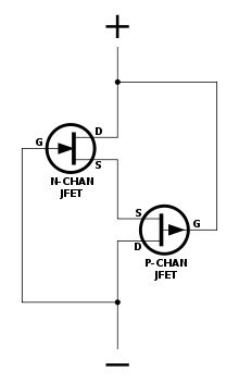
A lambda diode is an electronic circuit that combines a complementary pair of field-effect transistors into a two-terminal device that exhibits an area of differential negative resistance much like a tunnel diode. The term refers to the shape of the V–I curve of the device, which resembles the Greek letter λ (lambda).
Lambda diodes work at higher voltage than tunnel diodes. Whereas a typical tunnel diode[1] may exhibit negative differential resistance approximately between 70 mV and 350 mV, this region occurs approximately between 1.5 V and 6 V in a lambda diode due to the higher pinch-off voltages of typical JFET devices. A lambda diode therefore cannot replace a tunnel diode directly.
Moreover, in a tunnel diode the current reaches a minimum of about 20% of the peak current before rising again towards higher voltages. The lambda diode current approaches zero as voltage increases, before rising quickly again at a voltage high enough to cause gate–source Zener breakdown in the FETs.
It is also possible to construct a device similar to a lambda diode by combining an n-channel JFET with a PNP bipolar transistor.[2]
Applications
Like the tunnel diode, the negative resistance aspect of the lambda diode lends itself naturally to application in oscillator circuits[3] and amplifiers. In addition, bistable circuits such as memory cells have been described.[4]
References
- ↑ 1N3712 data sheet.
- ↑ Oscillations and Regenerative Amplification using Negative Resistance.
- ↑ A Dip Meter Using the Lambda Negative Resistance Circuit. Lloyd Butler, Amateur Radio, January 1997.
- ↑ United States Patent 4376986: Double Lambda diode memory cell; http://www.wipo.int/pctdb/images4/PCT-PAGES/1983/091983/83001335/83001335.pdf.
Literature
- Graf, Rudolf F. (1999). Modern Dictionary of Electronics, 7th ed. Boston [etc.]: Newnes Press. p. 411. ISBN 0-7506-9866-7.