Interband cascade laser
Interband cascade lasers (ICLs) are a type of laser diode that can produce coherent radiation over a large part of the mid-infrared region of the electromagnetic spectrum. They are fabricated from epitaxially-grown semiconductor heterostructures composed of layers of indium arsenide (InAs), gallium antimonide (GaSb), aluminum antimonide (AlSb), and related alloys. These lasers are similar to quantum cascade lasers (QCLs) in several ways. Like QCLs, ICLs employ the concept of bandstructure engineering to achieve an optimized laser design and reuse injected electrons to emit multiple photons. However, in ICLs, photons are generated with interband transitions, rather than the intersubband transitions used in QCLs. Consequently, the rate at which the carriers injected into the upper laser subband thermally relax to the lower subband is determined by interband Auger, radiative, and Shockley-Read carrier recombination. These processes typically occur on a much slower time scale than the longitudinal optical phonon interactions that mediates the intersubband relaxation of injected electrons in mid-IR QCLs. The use of interband transitions allows laser action in ICLs to be achieved at lower electrical input powers than is possible with QCLs.

The basic concept of an ICL was proposed by Rui Q. Yang in 1994.[1] The key insight he had was that the incorporation of a type-II heterostructure similar to those used in interband resonant tunneling diodes would facilitate the possibility of cascade lasers that use interband transitions for photon generation. Further improvement to the design and development of the technology was carried out by Yang and his collaborators at several institutions, as well as by groups at the Naval Research Laboratory and other institutions. ICLs lasing in continuous wave (cw) mode at room temperature were first demonstrated in 2008. This laser had an emission wavelength of 3.75 μm.[2] Subsequently, cw operation of ICLs at room temperature has been demonstrated with emission wavelengths ranging from 2.9 μm to 5.7 μm.[3] ICLs at cooler temperatures have been demonstrated with emission wavelengths between 2.7 μm to 11.2 μm.[4] ICLs operating in cw mode at ambient temperature are able to achieve lasing at much lower input powers than competing mid-IR semiconductor laser technologies.[5]
Theory of Operation

In a standard multiple quantum well laser, the active quantum wells used to generate photons are connected in parallel. Consequently, a large current is required to replenish each active well with electrons as it emits light. In a cascade laser, the wells are connected in series, meaning that the voltage is higher but the current is lower. This tradeoff is beneficial because the input power dissipated by the device's series resistance, Rs, is equal to I2Rs, where I is the electric current flowing through the device. Thus, the lower current in a cascade laser results in less power loss from the device's series resistance. However, devices with more stages tend to have poorer thermal performance, since more heat is generated in locations farther from the heat sink. The optimal number of stages depends on the wavelength, material used, and several other factors. The optimization of this number is guided by simulations, but ultimately determined empirically by studying the experimental laser performance.
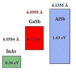
ICLs are fabricated from semiconductor heterostructures grown using molecular beam epitaxy (MBE). The materials used in the structure are InAs, GaSb, AlSb, and related alloys. These three binary materials are very closely lattice matched with lattice parameters close to 6.1 Å. Thus, these materials can be incorporated together in the same heterostructure without introducing a significant amount of strain. The MBE growth is typically done on either a GaSb or InAs substrate.
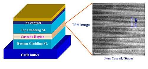
The entire epitaxial structure consists of several cascade stages that are sandwiched between two separate confinement layers (SCLs), with other materials enclosing the SCLs to provide optical cladding. In addition to producing light, the layered epitaxial structure must also act as a waveguide so that the cascade stages amplify guided optical modes.
Cascade Stage Design

In each cascade stage, the thin InAs layers act as confined quantum well (QW) layers for electrons and barriers for holes. The GaSb (or GaInSb) layers conversely act as QWs for holes and barriers for electrons, while the AlSb layers serve as barriers for both electrons and holes. The key feature that enables the realization of cascading within an interband diode is the so-called "type-II", or broken-gap, band alignment between InAs and GaSb. Whereas in the more usual class of type-I QWs both the electrons and holes are confined within the same material layer, the InAs-GaSb system is type-II because the conduction band minimum of InAs lies at a lower energy than the valence band maximum of GaSb. This less common arrangement makes it easy to re-inject electrons from the valence band of one stage of the ICL into the conduction band of the next stage via simple elastic scattering.
Each cascade stage effectively acts as an individual photon generator. A single stage is composed of an electron injector, a hole injector, and an active gain region consisting of one hole QW and one or two electron QWs.[6] When the device is biased, excess electrons and holes are generated and flow into the active region, where they recombine and emit light. In order to minimize optical losses at the semimetallic interface forming the boundary between the electron and hole injectors, a layer of AlSb is placed between the InAs and GaSb layers to prevent interband reabsorption of the generated photons.
A typical active region employs the so-called "W" quantum well configuration. In this design, the GaInSb hole QW is sandwiched between two InAs electron QWs, which are in turn surrounded by two AlSb barrier layers. This arrangement maximizes the optical gain by increasing the spatial overlap between the electron and hole wavefunctions that are nominally separated in different layers. The lasing wavelength, as determined by the bandgap created between the ground state electron and hole energy levels, can be varied simply by changing the InAs electron QW thickness (whereas it is much less sensitive to the hole QW thickness).
The two injector regions are each designed to efficiently transfer its namesake carriers (electrons or holes) from the semimetallic interface to the active region. They must also double as rectifying barriers for the opposite type of carrier in order to prevent inter-stage leakage currents. The total injector (electron injector plus hole injector) should also be sufficiently thick overall to prevent the electric fields forming under bias from becoming great enough to induce dielectric breakdown of the material. The electron injector is usually made longer because of the relatively fast inter-well scattering rate of electrons compared to that of holes. This ensures a smaller series resistance contribution from the total injector transport. The hole injector is composed of GaSb/AlSb quantum wells. It is made just thick enough (typically with just one or two wells) to ensure effective suppression of electron tunneling from the active region to the electron injector of the next stage. The electron injector typically consists of a longer series of InAs/AlSb quantum wells. To maximize the InAs/AlSb superlattice miniband width, the InAs layer thicknesses are varied across the injector so that their ground state energies nearly align when the device is biased. The quantum well energy gaps in the injector must be large enough to preclude reabsorption of the photons generated by the active quantum wells.
An additional feature that differentiates the ICL from all other laser diodes is its provision for electrically-pumped operation without a p-n junction. This is possible because the injectors function as rectifying barriers that keep the current flowing in a single direction. Nevertheless, it is highly advantageous to dope certain layers in each cascade stage as a means of controlling the active electron and hole densities, via a design technique called “carrier rebalancing.”[5] While the most favorable combination of electron and hole populations depends on the relative strengths of various free carrier absorption and Auger recombination processes, the studies done thus far indicate that the ICL performance is optimal when at threshold the two concentrations are roughly equal.[5] Since the hole population tends to substantially exceed the electron population in undoped or moderately-doped ICLs, carrier rebalancing is achieved by heavily n-doping the electron injector (typically, with Si) so as to add electrons to the active QWs.
Optical Waveguide
The gain within a given waveguide required to reach the lasing threshold is given by the equation:
where αwg is the waveguide loss, αmirr is the mirror loss, and Γ is the optical confinement factor. The mirror loss is due to photons escaping through the mirrors of the optical resonator. Waveguide losses can be due to absorption in the active, separate confinement, optical cladding materials, and metal contacts (if the claddings are not thick enough), or result from scattering at the ridge sidewalls. The confinement factor is that percentage of the optical energy concentrated in the cascade stages. As with other semiconductor lasers, ICLs have a tradeoff between optical loss in the waveguide and Γ. The overall goal of waveguide design is to find the proper structure that minimizes the threshold gain.
The choice of waveguide material depends on the substrate used. For ICLs grown on GaSb, the separate confinement layers are typically low-doped GaSb while the optical cladding layers are InAs/AlSb superlattices lattice-matched to the GaSb substrate. The bottom cladding must be fairly thick to prevent leakage of the guided mode into the substrate, since the refractive index of GaSb (about 3.8) is larger than the effective index of the lasing mode (typically 3.4-3.6).
An alternative waveguide configuration that is suitable for growth on InAs substrates uses highly n-doped InAs for the optical cladding.[7] The high electron density in this layer lowers the refractive index in accordance with the Drude model. In this approach, the epitaxial structure is grown on an n-type InAs substrate and it also utilizes InAs for the separate confinement layers. For longer-wavelength operation, advantages include the much higher thermal conductivity of bulk InAs as compared to a short-period InAs/AlSb superlattice, as well as a much thinner cladding layer due its larger index contrast with the active region. This shortens the MBE growth time, and also further improves the thermal dissipation. However, the waveguide must be designed carefully to avoid excessive free carrier absorption loss in the heavily-doped layers.
Current Status of ICL Performance

ICLs emitting at 3.7 um have operated in cw mode up to a maximum temperature of 118 °C.[8][9] A maximum cw output power of nearly 0.5 W has been demonstrated at room temperature, with 200-300 mW in a nearly-diffraction-limited beam. A maximum room-temperature cw wall-plug efficiency of nearly 15% has also been achieved. While QCLs typically require input electrical powers of nearly 1 W and higher to operate at room temperature, ICLs are able to lase for input powers as low as 29 mW owing to the much longer interband carrier lifetime.[5] Room-temperature cw operation with low dissipated powers can be achieved for wavelengths between approximately 3.0 um and 5.6 um.[3]
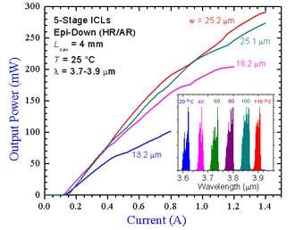
The figure on the right shows the performance characteristics of narrow ridge-waveguide interband cascade lasers at room temperature operating in cw mode.[8] Specifically, the figure shows plots of the amount of power emitted by lasers with different ridge widths for a given injection current. Each of these lasers had five cascade stages and cavity lengths of 4 mm. These lasers were mounted so that the top of the epitaxial structure (rather than the substrate) was in contact with the copper heat sink (typically referred to as an epitaxial side down configuration) in order to achieve optimal heat dissipation. In addition, they were fabricated with corrugated sidewalls. The sidewall corrugation lowers optical losses by ensuring fewer photons are generated in the higher-order optical modes that are more susceptible to optical scattering losses.
Applications
Mid-infrared lasers are important tools for spectroscopic sensing applications. Many molecules such as those in pollution and greenhouse gases have strong rotational and vibrational resonances in the mid-infrared region of the spectrum. For most sensing applications, the laser wavelength must also be within one of the atmospheric window to avoid signal attenuation.
An important requirement for this type of application is that single-mode emission is obtained. With ICLs, this can be done by making distributed feedback lasers. A distributed-feedback ICL,[10] designed for the excitation of methane gas, was developed at NASA Jet Propulsion Laboratory and included as an instrument on the tunable laser spectrometer on the Curiosity rover that was sent to explore the environment of Mars. A more recent distributed feedback ICL emitted up to 27 mW in a single spectral mode at 3.79 μm when operated at 40 °C, and 1 mW for operation at 80 °C.[11]
References
- ↑ Yang, R. Q. (1995). "Infrared Laser based on Intersubband Transitions in Quantum Wells". Superlattices and Microstructures. 17 (1): 77–83. Bibcode:1995SuMi...17...77Y. doi:10.1006/spmi.1995.1017.
- ↑ Kim, M.; C.L. Canedy; W.W. Bewley; C.S. Kim; J.R. Lindle; J. Abell; I. Vurgaftman; J.R. Meyer (2008). "Interband cascade laser emitting at λ = 3.75 μm in continuous wave above room temperature". Applied Physics Letters. 92: 191110. Bibcode:2008ApPhL..92s1110K. doi:10.1063/1.2930685.
- 1 2 Bewley, W.W.; C.L. Canedy; C.S. Kim; M. Kim; C.D. Merritt; J. Abell; I. Vurgaftman; J.R. Meyer (2012). "Continuous-wave interband cascade lasers operating above room temperature at λ = 4.7-5.6 μm". Optics Express. 20: 3235–3240. Bibcode:2012OExpr..20.3235B. doi:10.1364/OE.20.003235.
- ↑ Li, L.; H. Ye; Y. Jiang; R.Q. Yang; J. C. Keay; T.D. Mishima; M.B. Santos; M.B. Johnson (2015). "MBE-grown long-wavelength interband cascade lasers on InAs substrates". J. Cryst. Growth. 426: 369. doi:10.1016/j.jcrysgro.2015.02.016.
- 1 2 3 4 Vurgaftman, I.; W.W. Bewley; C.L. Canedy; C.S. Kim; M. Kim; C.D. Merritt; J. Abell; J.R. Lindle; J.R. Meyer (2011). "Rebalancing of internally generated carriers for mid-infrared cascade lasers with very low power consumption". Nature Communications. 2: 585. Bibcode:2011NatCo...2E.585V. PMID 22158440. doi:10.1038/ncomms1595.
- ↑ Vurgaftman, I.; W.W. Bewley; C.L. Canedy; C.S. Kim; M. Kim; J.R. Lindle; C.D. Merritt; J. Abell; J.R. Meyer (2011). "Mid-IR Type-II Interband Cascade Lasers". IEEE Journal of Selected Topics in Quantum Electronics. 17 (5): 1435–1444. doi:10.1109/JSTQE.2011.2114331.
- ↑ Tian, Z.; R.Q. Yang; T.D. Mishima; M.B. Santos; R.T. Hinkey; M.E. Curtis; M.B. Johnson (2008). "InAs-based interband cascade lasers near 6 μm". Electronics Letters. 45: 48–49. doi:10.1049/el:20092779.
- 1 2 Bewley, W.W.; C.L. Canedy; C.S. Kim; M. Kim; C.D. Merritt; J. Abell; I. Vurgaftman; J.R. Meyer (2012). "High-power room-temperature continuous-wave mid-infrared interband cascade lasers". Optics Express. 20: 20894–20901. Bibcode:2012OExpr..2020894B. doi:10.1364/OE.20.020894.
- ↑ Vurgaftman, I.; R. Weih; M. Kamp; J.R. Meyer; C.L. Canedy; M. Kim; W.W. Bewley; C.D. Merritt; J. Abell; S. Hoefling (2015). "Topical Review - Interband cascade lasers". Journal of Physics D: Applied Physics. 48: 123001–123017. Bibcode:2015JPhD...48l3001V. doi:10.1088/0022-3727/48/12/123001.
- ↑ Yang, R.Q.; C.J..Hill; K. Mansour; Y. Qiu; A. Soibel; R.E. Muller; P.M. Echternach (2007). "Distributed Feedback Mid-IR Interband Cascade Lasers at Thermoelectric Cooler Temperatures". IEEE Journal of Selected Topics in Quantum Electronics. 13: 1074–1078. doi:10.1109/JSTQE.2007.903014.
- ↑ Kim, C.S.; M. Kim; J. Abell; W.W. Bewley; C.D. Merritt; C.L. Canedy; I.Vurgaftman; J.R. Meyer (2012). "Mid-IR Distributed-Feedback Interband Cascade Lasers with Continuous-Wave Single-Mode Emission to 80 °C.". Applied Physics Letters. 101: 061104. Bibcode:2012ApPhL.101f1104K. doi:10.1063/1.4744445.