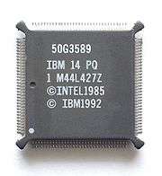
IBM 386SLC
The 386SLC was an Intel-licensed version of the 386SX (32-bit internal, 16-bit external, 24-bit memory addressing), developed and manufactured by IBM in 1991. It included power-management capabilities and an 8KB internal CPU cache, which enabled it to yield comparable performance to 386DX processors of the same clock speed, which were considerably more expensive. Known inside IBM as "Super Little Chip" for its initials, it was used in IBM PS/2 35, 40 56 Series and in the IBM PS/ValuePoint 325T, but never gained much market share. This was mainly due to an agreement with Intel, in which IBM was not allowed to sell their CPUs if they were not part of a system or upgrade board. It was also marketed as an optional upgrade for 8086-equipped IBM PS/2 25 Series computers.
Design and Technology
Built with complementary metal oxide semiconductor (CMOS) technology, the IBM 386SLC had a 161-square millimeter die. It was available with clock speeds of 16, 20, and 25 MHz. The 25 MHz model produced only 2.5 watts of dissipated power, making it specially well suited for laptops and other portable devices.
Despite the fact that the SLC and DLC chips are bus compatible with i386SX and i386DX respectively, they can not be used as drop-in replacements as they are not pin-compatible.
IBM 486SLC
Is an improved version of the IBM 386SLC, based on the Intel core. IBM 486SLC featured 16Kb of L1 cache and the i486 instruction set. It had 1.349 mln. transistors and a 69mm² die. It was manufactured in 1992. It came in a 100-pin PQFP packge, with 33 MHz FSB speed. The 486SLC was also available in a clock-doubled version, the 486SLC2 (50,66 MHz), and later in a clock tripled-version, the 486SLC3 (60,75,100 MHz). Clock-for-clock, it was substantially faster than the similarly-named Cyrix part, yielding performance broadly comparable to a similarly-clocked 486SX in the 16-bit applications of its day. However, its narrow 16-bit bus, limited memory addressing capability (16 MB) and lack of on-chip FPU would prove to be major disadvantages under the new generation of 32-bit operating systems (such as Windows 95) that would become popular in following years.
It is suspected the clock tripled 486SLC3 part did not in fact actually exist as a stand-alone product. All known instances of 486SLC3 CPUs are reportedly in the 132pin PQFP packaging with the extra address lines not connected (a 486BL3 running in 16-bit mode).
IBM 486DLC (Blue Lightning)

The 486DLC is a fully 32-bit version of the 486SLC, with 1.4 mln transistors on the 82mm² die and 0.8 µm CMOS. It came in a 132-pin QFP package. In July, 1993 IBM produced clock-doubled and clock-tripled versions of the chip, the 486DLC2 (486BLX2) and the 486DLC3 (486BLX3) respectively. The chips were available from 50 to 100 MHz and were sold by IBM only.

IBM later marketed Socket 3 168-pin PGA Blue Lightning 486 CPUs, but these are technically not related to earlier Blue Lightning models as they are based on the Cyrix Cx486 CPU core.
See also
- Intel 386
- IBM PS/2
- IBM PS/ValuePoint
- IBM ThinkPad
- IBM 5x86C - based on the Cyrix core
- IBM Personal Computer