Heterostructure-emitter bipolar transistor
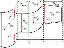
The Heterojunction-emitter bipolar transistor (HEBT), is a somewhat unusual arrangement with respect to emitter blocking of minority carriers. This is accomplished by using heterostructure confinement in the emitter, introducing an energy barrier to minority-carrier charge flow from the base. This is important as loss of minority carriers from the base to the emitter degrades analog performance. The main difference of the HEBT from the Heterojunction bipolar transistor (HBT) is that the emitter–base interface is the same as in a bipolar junction transistor (BJT) with the blocking energy gap being moved back into the emitter bulk region.
Functional Architecture

The main advantage of HEBT architecture, compared to the HBT is a simplified fabrication process for the emitter–base junction. In particular the HEBT does not require as tight parametric control during epitaxial growth, that equivalent abrupt or graded emitter structures might. This is very important as it is evident from scanning ion mass spectrometry data that out-diffusion base dopant into the emitter junction is difficult to control, as the base is, in general, very highly doped in order to enhance performance.
Application
The HEBT is well positioned as a potential candidate for key roles in high-frequency optoelectronic markets, similar to the Heterojunction bipolar transistor. Also of importance for optoelectronic hybrids is that HEBT can be constructed in any semiconductor system that permits the use of band-gap–altering alloys in the emitter.
References
- Rutherford, William C. (1994). "Comparative modelling of current gain and cutoff frequency for heterostructure confinement and heterojunction bipolar transistors". Solid-State Electronics. 37 (10): 1783. doi:10.1016/0038-1101(94)90231-3.
- Cheng, Shiou-Ying (2002). "Theoretical investigation of an InGaP/GaAs heterostructure-emitter bipolar transistor with a wide-gap collector". Semiconductor Science and Technology. 17 (5): 405. doi:10.1088/0268-1242/17/5/301.