Ernst Ruska-Centre
 | |
| Abbreviation | ER-C |
|---|---|
| Motto | Physics is our Profession |
| Predecessor | none |
| Successor | n/a |
| Established | 27 January 2004 |
| Type | Research Laboratory |
| Headquarters | Jülich |
| Location | |
| Coordinates | 50°54′29″N 6°24′49″E / 50.90806°N 6.41361°ECoordinates: 50°54′29″N 6°24′49″E / 50.90806°N 6.41361°E |
Region served | Worldwide |
Official language | German and English |
Directors | Rafal E. Dunin-Borkowski and Joachim Mayer |
Founding Direct. | Knut Urban |
General Manager | Karsten Tillmann |
Section Leaders | Michael Feuerbacher, Lothar Houben, Chunlin Jia, Martina Luysberg, Andreas Thust |
Main organ | Contractual Partners Assembly |
| Affiliations | Jülich Research Centre and RWTH Aachen University |
Staff | 40 |
| Website |
www |
The Ernst Ruska-Centre (ER-C) for Microscopy and Spectroscopy with Electrons is a German research establishment conjointly operated by the Jülich Research Centre and RWTH Aachen University on a pari passu basis. The facility, which also offers user services to external research groups, is located on the campus of Research Centre Jülich belonging to the Helmholtz Association of German Research Centres.
The ER-C's main purposes are fundamental research in high-resolution transmission electron microscopy method development as well as respective applications coming along with topical problems in solid state research and energy research. For theses purposes the ER-C runs several state-of-the-art transmission electron microscopes and develops customed software solutions to be used for e.g. for the exit wave retrieval purposes or the measurement of higher-order lens aberrations.
The ER-C was founded in Aachen on 27 January 2004[1] by means of a contract signed by the chairman of Forschungszentrum Jülich Joachim Treusch and RWTH Aachen University's rector Burkhard Rauhut. The centre was inaugurated on 18 May 2006 in presence of members of the Ernst Ruska family as well as representatives of the international electron microscopy community.[2]
Instrumental Resources

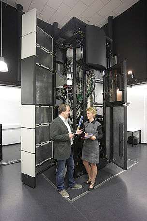
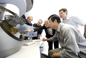
The ER-C presently houses 13 electron microscopes manufactured by FEI Company and JEOL Ltd. ranging from standard scanning electron microscopes to highly specialised Titan series transmission electron microscopes equipped with aberration correction units and offering an information limit well below 100 picometres. The majority of ER-C instrumental resources is available for use by both in-house and external users.

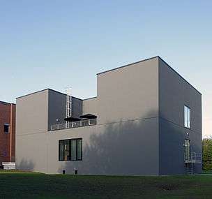
On 12 December 2008 the ER-C and FEI Company announced that a next generation electron microscope with a record resolution of 50 picometres will be made available to a broad user community from 2010.[3] The instrument known as PICO, which is equipped with a special unit allowing for the correction of the chromatical aberration for the first time in electron microcopy,[4] allows to see details measuring only a fraction of an atomic diameter and thus at the absolute limits of optical systems. This enables atomic structures for materials in energy research and microelectronics to be investigated more precisely than has ever been possible before. On 4 November 2009 work began on an extension to the ER-C to house the PICO microscope with a groundbreaking ceremony[5] and the building was formally inaugurated on 29 September 2011. The PICO microscope was inaugurated on 29 February 2012.[6]
Research Programmes

Focal points of inherent ER-C research programmes cover the scrutineering of, both, the theoretical and the applied aspects of high-resolution transmission electron microscopy, which in turn represents the most important analysis methods at the centre. Numerical software packages largely developed by ER-C scientists and allowing for the retrieval of the exit plane wavefunction together with the precise control of higher order lens aberrations are in use globally in a continuously increasing number of electron microscopy laboratories.
Present in-house materials science research projects focus on the investigation of the epitaxial growth mechanisms and the relaxation behaviour of nanostructured material combinations by software-based methods of transmission electron microscopy. Relevant research projects comprise high-precision measurements of atomic spacings down to a few picometres,[7] the identification of novel relaxation mechanisms together with the quantification of individual contributions towards the reduction of elastic stresses in lattice strained heterostructures, the quantification of interdiffusion related parameters in multilayer systems on the atomic scale as well as the measurement of dopant induced electrical fields by means of electron holography techniques. Material classes investigated include nanostructured electroceramics, complex metallic alloys, semiconductor materials and oxide superconductors together with lattice defects by advanced techniques electron microscopy.
References
- ↑ Press Release: Foundation of the Ernst Ruska-Centre
- ↑ Press Release: Inauguration of the Ernst Ruska-Centre
- ↑ Press Release: Globally most Powerful Microscope to be Installed in Jülich
- ↑ Animation: PICO - How it works
- ↑ Press Release: Work Begins on Laboratory for World's Most Powerful Electron Microscope
- ↑ Press Release: PICO - Unique electron microscope inaugurated
- ↑ Press Release: Electron Microscopy Enters the Picometre Scale
External links
- Ernst Ruska-Centre for Microscopy and Spectroscopy with Electrons (ER-C)
- Ernst Ruska-Centre for Microscopy and Spectroscopy with Electrons (ER-C), Staff
- Webservices of Forschungszentrum Jülich (JÜLICH)
- Webservices of RWTH Aachen University (RWTH)
- Webservices of German Research Foundation (DFG)