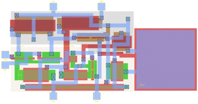
Integrated circuit layout

Integrated circuit layout, also known IC layout, IC mask layout, or mask design, is the representation of an integrated circuit in terms of planar geometric shapes which correspond to the patterns of metal, oxide, or semiconductor layers that make up the components of the integrated circuit.
When using a standard process - where the interaction of the many chemical, thermal, and photographic variables are known and carefully controlled - the behaviour of the final integrated circuit depends largely on the positions and interconnections of the geometric shapes. Using a computer-aided layout tool, the layout engineer—or layout technician—places and connects all of the components that make up the chip such that they meet certain criterion—typically: performance, size, density, and manufacturability. This practice is often subdivided between two primary layout disciplines: Analog and Digital.
The generated layout must pass a series of checks in a process known as physical verification. The most common checks in this verification process are[1]
- design rule checking (DRC),
- layout versus schematic (LVS),
- parasitic extraction,
- antenna rule checking, and
- electrical rule checking (ERC).
When all verification is complete, the data is translated into an industry standard format, typically GDSII, and sent to a semiconductor foundry. The process of sending this data to the foundry is called tapeout due to the fact the data used to be shipped out on a magnetic tape. The foundry converts the data into another format and uses it to generate the photomasks used in a photolithographic process of semiconductor device fabrication.
In the earlier, simpler, days of IC design, layout was done by hand using opaque tapes and films, much like the early days of PCB design. Modern IC layout is done with the aid of IC layout editor software, mostly automatically using EDA tools, including place and route tools or schematic driven layout tools. The manual operation of choosing and positioning the geometric shapes is informally known as "polygon pushing".
See also
References
- ↑ A. Kahng, J. Lienig, I. Markov, J. Hu: VLSI Physical Design: From Graph Partitioning to Timing Closure, ISBN 978-90-481-9590-9, p. 10.
Further reading
- Saint, Christopher and Judy. (2002). IC Layout Basics. McGraw-Hill. ISBN 0-07-138625-4
- Clein, Dan. (2000). CMOS IC Layout. Newnes. ISBN 0-7506-7194-7
- Hastings, Alan. (2005). The Art of Analog Layout. Prentice Hall. ISBN 0-13-146410-8