Organic photorefractive materials
Organic photorefractive materials are materials that exhibit a temporary change in refractive index when exposed to light. The changing refractive index causes light to change speed throughout the material and produce light and dark regions in the crystal. The buildup can be controlled to produce holographic images for use in biomedical scans and optical computing. The ease with which the chemical composition can be changed in organic materials makes the photorefractive effect more controllable.
History
Although the physics behind the photorefractive effect were known for quite a while, the effect was first observed in 1967 in LiNbO3.[1] For more than thirty years, the effect was observed and studied exclusively in inorganic materials, until 1990, when a nonlinear organic crystal 2-(cyclooctylamino)-5-nitropyridine (COANP) doped with 7,7,8,8-tetracyanoquinodimethane (TCNQ) exhibited the photorefractive effect.[1] Even though inorganic material-based electronics dominate the current market, organic PR materials have been improved greatly since then and are currently considered to be an equal alternative to inorganic crystals.[2]
Theory
There are two phenomena that, when combined together, produce the photorefractive effect. These are photoconductivity, first observed in selenium by Willoughby Smith in 1873,[3] and the Pockels Effect, named after Friedrich Carl Alwin Pockels who studied it in 1893.[4]
Photoconductivity is the property of a material that describes the capability of incident light of adequate wavelength to produce electric charge carriers. The Fermi level of an intrinsic semiconductor is exactly in the middle of the band gap. The densities of free electrons n in the conduction band and free holes h in the valence band can be found through equations:[5]

and

where NC and NV are the densities of states at the bottom of the conduction band and the top of the valence band, respectively, EC and EV are the corresponding energies, EF is the Fermi level, kB is Boltzmann’s constant and T is the absolute temperature. Addition of impurities into the semiconductor, or doping, produces excess holes or electrons, which, with sufficient density, may pin the Fermi level to the impurities’ position.[6]
A sufficiently energetic light can excite charge carriers so much that they will populate the initially empty localized levels. Then, the density of free carriers in the conduction and/or the valence band will increase. To account for these changes, steady-state Fermi levels are defined for electrons to be EFn and, for holes – EFp. The densities n and h are, then equal to


The localized states between EFn and EFp are known as ‘photoactive centers.’ The charge carriers remain in these states for a long time until they recombine with an oppositely charged carrier. The states outside the EFn – EFp energy, however, relax their charge carriers to the nearest extended states.[5]
The effect of incident light on the conductivity of the material depends on the energy of light and material. Differently-doped materials may have several different types of photoactive centers, each of which requires a different mathematical treatment. However, it is not very difficult to show the relationship between incident light and conductivity in a material with only one type of charge carrier and one type of a photoactive center. The dark conductivity of such a material is given by

where σd is the conductivity, e = electron charge, ND and ND+ are the densities of total photoactive centers and ionized empty electron acceptor states, respectively, β is the thermal photoelectron generation coefficient, μ is the mobility constant and τ is the photoelectron lifetime.[5] The equation for photoconductivity substitutes the parameters of the incident light for β and is

in which s is the effective cross-section for photoelectron generation, h is the Planck constant, ν is the frequency of incident light, and the term I = I0e-αz in which I0 is the incident irradiance, z is the coordinate along the crystal thickness and α is the light intensity loss coefficient.[5]
The electro-optic effect is a change of the optical properties of a given material in response to an electric field. There are many different occurrences, all of which are in the subgroup of the electro-optic effect, and Pockels effect is one of these occurrences. Essentially, the Pockels effect is the change of the material’s refractive index induced by an applied electric field. The refractive index of a material is the factor by which the phase velocity is decreased relative to the velocity of light in vacuum. At a microscale, such a decrease occurs because of a disturbance in the charges of each atom after being subjected to the electromagnetic field of the incident light. As the electrons move around energy levels, some energy is released as an electromagnetic wave at the same frequency but with a phase delay. The apparent light in a medium is a superposition of all of the waves released in such way, and so the resulting light wave has shorter wavelength but the same frequency and the light wave’s phase speed is slowed down.[7]
Whether or not the material will exhibit Pockels effect depends on its symmetry. Both centrosymmetric and non-centrosymmetric media will exhibit an effect similar to Pockels, the Kerr effect. The refractive index change will be proportional to the square of the electric field strength and will therefore be much weaker than the Pockels effect. It is only the non-centrosymmetric materials that can exhibit the Pockels effect: for instance, lithium tantalite (trigonal crystal) or gallium arsenide (zinc-blende crystal); as well as poled polymers with specifically designed organic molecules.[8]
It is possible to describe the Pockels effect mathematically by first introducing the index ellipsoid – a concept relating the orientation and relative magnitude of the material’s refractive indices. The ellipsoid is defined by

in which εi is the relative permittivity along the x, y, or z axis, and R is the reduced displacement vector defined as Di/√8πW in which Di is the electric displacement vector and W is the field energy. The electric field will induce a deformation in Ri as according to:

in which E is the applied electric field, and rij is a coefficient that depends on the crystal symmetry and the orientation of the coordinate system with respect to the crystal axes. Some of these coefficients will usually be equal to zero.[7]
Organic Photorefractive Materials

In general,photorefractive materials can be classified into the following categories, the border between categories may not be sharp in each case
- Inorganic crystal and compound semiconductor
- Multiple quantum well structures
- Organic crystalline materials
- Polymer dispersed Liquid crystalline materials (PDLC)
- Organic amorphous materials

In the field of this research, initial investigations were mainly carried out with inorganic semiconductors. There have been huge varieties of inorganic crystals such as BaTiO3, KNbO3, LiNbO3 and inorganic compound semiconductors such as GaAs, InP, CdTe are reported in literature.[9] First photorefractive(PR) effect in organic materials was reported in 1991 and then, research of organic photorefractive materials has drawn major attention in recent years compare to inorganic PR semiconductors. This is due to mainly cost effectiveness, relatively easy synthetic procedure, and tunable properties through modifications of chemical or compositional changes.
Polymer or polymer composite materials have shown excellent photorefractive properties of 100% diffraction efficiency. Most recently, amorphous composites of low glass transition temperature have emerged as highly efficient PR materials. These two classes of organic PR materials are also mostly investigated field. These composite materials have four components -conducting materials, sensitizer, chromophore, and other dopant molecules to be discussed in terms of PR effect. According to the literature,design strategy of hole conductors is mainly p-type based [10] and the issues on the sensitizing are accentuated on n-type electron accepting materials, which are usually of very low content in the blends and thus do not provide a complementary path for electron conduction. In recent publications on organic PR materials, it is common to incorporate a polymeric material with charge transport units in its main or side chain. In this way, the polymer also serves as a host matrix to provide the resultant composite material with a sufficient viscosity for reasons of processing. Most guest-host composites demonstrated in the literature so far are based on hole conducting polymeric materials.
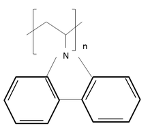
The vast majority of the polymers are based on carbazole containing polymers like poly-(N-vinyl carbazole) (PVK) and polysiloxanes (PSX). PVK is the well studied system for huge varieties of applications.[11] In polymers,charge is transported through the HOMO and the mobility is influenced by the nature of the dopant mixed into the polymer, also it depends on the amount of dopant which may exceed 50 weight percent of the composite for guest-host materials.[12] The mobility decreases as the concentration of charge-transport moieties decreases, and the dopant’s polarity and concentration increases.[13]
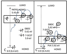
Besides the mobility, the ionization potential of the polymer and the respective dopant has also significant importance. The relative position of the polymer HOMO with respect to the ionization potential of the other components of the blends determines the extent of extrinsic hole traps in the material.[14] TPD (tetraphenyldiaminophenyl) based materials are known to exhibit higher charge carrier mobilities and lower ionization potentials compare to carbazole based (PVK) materials. The low ionization potentials of the TPD based materials greatly enhance the photoconductivity of the materials. This is partly due to the enhanced complexation of the hole conductor, which is an electron donor, with the sensitizing agents, which is an electron acceptor. It was reported a dramatic increase of the photogeneration efficiency from 0.3% to 100% by lowering the ionization potential from 5.90 eV (PVK) to 5.39 eV ( TPD derivative PATPD).[15] This is schematically explained in the diagram using the electronic states of PVK and PATPD.
Applications
As of 2011, no commercial products utilizing organic photorefractive materials exist.[2] All applications described are speculative or performed in research laboratories. Large DC fields required to produce holograms lead to dielectric breakdown not suitable outside the laboratory.
Reusable Holographic Displays

Many materials exist for recording static, permanent holograms including photopolymers, silver halide films, photoresists, dichromated gelatin, and photorefractives. Materials vary in their maximum diffraction efficiency, required power consumption, and resolution. Photorefractives have a high diffraction efficiency, an average-low power consumption, and a high resolution.
Updatable holograms that do not require glasses are attractive for medical and military imaging. The materials properties required to produce updatable holograms are 100% diffraction efficiency, fast writing time, long image persistence, fast erasing time, and large area.[16] Inorganic materials capable of rapid updating exist but are difficult to grow larger than a cubic centimeter. Liquid crystal 3D displays exist but require complex computation to produce images which limits their refresh rate and size.
Blanche et al. demonstrated in 2008 a 4 in. x 4 in. display that refreshed every few minutes and lasted several hours.[17] Organic photorefractive materials are capable of kHz refresh rates though it is limited by material sensitivity and laser power. Material sensitivity demonstrated in 2010 require kW pulsed lasers.[18]
Tunable Color Filter
White light passed through an organic photorefractive diffraction grating, leads to the absorption of wavelengths generated by surface plasmon resonance and the reflection of complementary wavelengths. The period of the diffraction grating may be adjusted by modifying to control the wavelengths of the reflected light. This could be used for filter channels, optical attenuators, and optical color filters[19]
Optical communications
Free-space optical communications(FSO) can be used for high-bandwidth communication of data by utilizing high frequency lasers. Phase distortions created by the atmosphere can be corrected by a four-wave mixing process utilizing organic photorefractive holograms.[20] The nature of FSO allows images to be transmitted at near original quality in real-time.[21] The correction also corrects for moving images.[21]
Image and Signal Processing
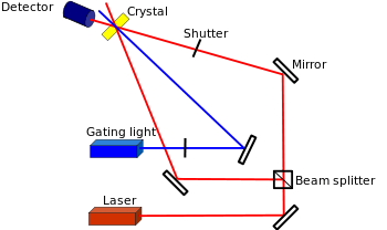
Organic photorefractive materials are a nonlinear medium in which large amounts of information can be recorded and read.[22] Holograms due to the inherent parallel nature of optical recording are able to quickly process large amounts of data. Holograms that can be quickly produced and read can be used to verify the authenticity of documents similar to a watermark[22] Organic photorefractive correlators use matched filter[23] and Joint Fourier Transform[24] configurations.
Logical functions (AND, OR, NOR, XOR, NOT) were carried out using two-wave signal processing.[25] High diffraction efficiency allowed a CCD detector to distinguish between light pixels (1 bits) and dark pixels (0 bits).[25]
References
- 1 2 Moerner, W. E.; Silence, Scott M. (1994). "Polymeric photorefractive materials". Chemical Reviews 94 (1): 127–155. doi:10.1021/cr00025a005. ISSN 0009-2665.
- 1 2 Köber, S.; Salvador, M.; Meerholz, K (2011). "Organic Photorefractive Materials and Applications". Advanced Materials 23: 4725–4763. doi:10.1002/adma.201100436.
- ↑ Smith, Willoughby (20 February 1873). "Effect of Light on Selenium during the passage of an Electric Current". Nature: 303. Bibcode:1873Natur...7R.303.. doi:10.1038/007303e0.
- ↑ Burland, Donald (January 1994). "Optical Nonlinearities in Chemistry: Introduction". Chem. Rev. (94 (1)): 1–2. doi:10.1021/cr00025a600.
- 1 2 3 4 Frejlich, Jaime (2007). Photorefractive Materials: Fundamental Concepts, Holographic Recording and Materials Characterization. WILEY-INTERSCIENCE. ISBN 978-0-471-74866-3.
- ↑ Joshi, N.V. (1990). Photoconductivity: art, science, and technology. CRC Press. ISBN 978-0-8247-8321-1.
- 1 2 Paschotta, Rüdiger. "Encyclopedia of Laser Physics and Technology".
- ↑ Paschotta, Rüdiger. "Encyclopedia of Laser Physics and Technology".
- ↑ K. Buse , J. Imbrock , E. Krätzig , K. Peithmann , in Photorefractive Materials and Their Applications II: Materials (Eds: P. Günter ,J. P. Huignard ), Springer Series In Optical Science , Vol. 114 , Springer , Berlin 2006 , 83–121
- ↑ K. Meerholz , B. L. Volodin , B. Kippelen , N. Peyghambarian , Nature 1994 , 371 , 497–500
- ↑ M. B. Klein , in Photorefractive Materials and Their Applications II: Materials (Eds: P. Günter , J. P. Huignard ), Springer Series In Optical Science , Vol. 114 , Springer , Berlin 2006 , 241–284
- ↑ M. Angiuli , F. Ciardelli , A. Colligiani , F. Greco , A. Romano ,G. Ruggeri , E. Tombari , Appl. Opt. 2006 , 45 , 7928–7937
- ↑ J. A. Herlocker , C. Fuentes-Hernandez , K. B. Ferrio , E. Hendrickx ,P.-A. Blanche , N. Peyghambarian , B. Kippelen , Y. Zhang , J. F. Wang ,S. R. Marder , Appl. Phys. Lett. 2000 , 77 , 2292–2294
- ↑ J. Thomas , C. Fuentes-Hernandez , M. Yamamoto , K. Cammack , K. Matsumoto , G. A. Walker , S. Barlow , B. Kippelen , G. Meredith , S. R. Marder , N. Peyghambarian , Adv. Mater. 2004 , 16 , 2032–2036
- ↑ E. Hendrickx , B. Kippelen , S. Thayumanavan , S. R. Marder , A. Persoons , N. Peyghambarian , Chem. Phys. 2000 , 112 ,9557–9561
- ↑ Tay,S.A.; Blanche, P.A. "An updateable holographic three-dimensional display". Nature 451: 694–698. Bibcode:2008Natur.451..694T. doi:10.1038/nature06596.
- ↑ Blanche,P.A.; Tay,S. "An Updatable Holographic Three-Dimensional Display for 3D Visualization". Journal of Display Technology 4: 424–430. doi:10.1109/jdt.2008.2001574.
- ↑ Blanche,P.A.; Bablumian,A. "Future of Photorefractive based Holographic 3D display". Proc. SPIE: 7619.
- ↑ Oh, J.; Choi, J. "Tunable color filter with surface plasmon resonance using organic photorefractive composite". Optics InfoBase 48: 3160. Bibcode:2009ApOpt..48.3160O. doi:10.1364/ao.48.003160.
- ↑ Li, G.; Eralp, M. (2005). "All-optical dynamic correction of distorted communication signals using a photorefractive polymeric hologram". Appl. Phys. Lett. 86: 161103. Bibcode:2005ApPhL..86p1103L. doi:10.1063/1.1898432.
- 1 2 Winiarz, J.; Ghebremichael, F.; Thomas, J. "Dynamic correction of a distorted image using a photorefractive polymer composite" 12: 2517–2528.
- 1 2 Volodin, B.L.; Kippelen, B. "A polymeric optical pattern recognition system for security verification". Nature 383 (6595): 58–60. Bibcode:1996Natur.383...58V. doi:10.1038/383058a0.
- ↑ Halvorson, C.; Kraabel, B. (1995). "Optical computing by use of photorefractive polymers" 20: 76–78.
- ↑ Banerjee, P.P.; Gad, E. "Edge Enhancement and Edge-Enhanced Correlation with Photorefractive Polymers" 39: 5337–5346.
- 1 2 Ishikawa, D.; Okamoto, A. "All-Optical Multifunctional Logic Gates for Image Information Using Photorefractive Two-Wave Mixing" 14: 246–251.