Tensilica
| Subsidiary | |
| Industry | Semiconductor intellectual property core |
| Founded | 1997 |
| Headquarters | San Jose, California |
Key people | Chris Rowen, Jack Guedj, Martin Lund |
| Products | Microprocessors, Hifi audio, DSP cores |
| Website |
ip |
Tensilica is a company based in Silicon Valley in the semiconductor intellectual property core business. It is now a part of Cadence Design Systems. Its dataplane processors (DPUs) bring together the strengths of CPUs and DSPs and custom logic with 10× to 100× the performance, making them suited for data-intensive processing tasks.
The Tensilica brand is best known for its customizable microprocessor core, the Xtensa configurable processor. Other products include: HiFi audio/voice DSPs with a software library of over 125 codecs from Cadence and over 55 software partners; IVP Image/Video DSP, designed to handle complex algorithms in imaging, video and computer vision; and ConnX family of baseband DSPs ranging from the dual-MAC ConnX D2 to the 64-MAC ConnX BBE64EP.
Tensilica was founded in 1997 by Chris Rowen (one of the founders of MIPS Technologies) and was initially staffed by former employees of several other Silicon Valley processor and electronic design automation companies. It employed Earl Killian, who contributed to the MIPS instruction set, as chief software architect for several years.[1] On March 11, 2013, Cadence Design Systems announced its intent to buy Tensilica for approximately $380 million in cash.[2] Cadence completed the acquisition in April 2013, with a cash outlay at closing of approximately $326 million. The Tensilica team, led by Jack Guedj, reports to Martin Lund, who is Cadence's senior vice president of its IP Group.[3]
Cadence Tensilica products
Cadence Tensilica develops SIP blocks to be included on the dies of products of their licensee's, such as System on a chips for embedded systems, particularly in mobile, home entertainment, and communications.
Xtensa configurable cores
An Xtensa DPU (data plane processing unit) can be employed as anything from a small, low-power cache-less microcontroller to a high-performance 16-way SIMD, 3-issue VLIW DSP core.
IP processor vendors such as Tensilica typically offer their licensees the choice between many of the IP core's implementation details: cache size, processor bus width, data and instruction RAMs, memory management and interrupt control. However, Cadence's Xtensa architecture offers a key differentiating feature, a user-customizable instruction set.
Using the supplied customization tools, customers can extend the Xtensa base instruction set by adding new user-defined instructions. Extensions can include SIMD instructions, new register files, and additional data transfer interfaces for multiprocessor communication. After the final processor configuration is made and submitted, Cadence's processor generator service builds the configured Xtensa IP core, processor design kit, and software development kit. This process is highly automated so designers can quickly experiment with different instruction additions, testing the performance improvements and power trade-offs of the various alternatives.
The processor kit contains items necessary to integrate the configured IP into the customer's chip design environment: the core's hardware description (in synthesizeable RTL or physical post-layout form), timing & I/O constraints, requirements for technology-specific RAMs/caches/FIFOs. The software kit is built on the Eclipse-based integrated development environment, and uses a GNU Compiler Collection-derived tool-chain: C/C++ compiler, assembler, linker, debugger. An instruction set simulator enables customers to begin application development before actual hardware is available.
Xtensa instruction set
The Xtensa instruction set is designed to meet the diverse requirements of dataplane processing. This 32-bit architecture features a compact 16- and 24-bit instruction set with modeless switching for maximum power efficiency and performance. The base instruction set has 80 RISC instructions and includes a 32-bit ALU, up to 64 general-purpose 32-bit registers, and six special-purpose registers. Using this instruction set, you can expect significant code size reductions that result in higher code density and better power dissipation.
Adoption
AMD's TrueAudio and Unified Video Decoder are ASICs based on Xtensa.
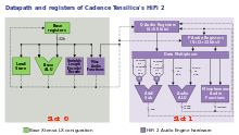
HiFi Audio and Voice DSP IP

- HiFi Mini Audio DSP — Our smallest, lowest power DSP core for always-listening voice trigger and voice recognition
- HiFi 2 Audio DSP — This highly efficient DSP core provides the lowest power MP3 audio processing
- HiFi EP Audio DSP — A superset of HiFi 2 with advanced optimizations for DTS Master Audio, improved voice pre- and post-processing, and improved cache memory subsystem
- HiFi 3 Audio DSP — Full 32-bit processing makes this DSP super efficient for many of the audio enhancement algorithms, wideband voice codecs, and multi-channel audio
Adoption
AMD TrueAudio, found e.g. in the PlayStation 4, in "Kaveri" desktop APUs and in a very few of AMD's graphics cards, is based on the Cadence Tensilica HiFi EP Audio DSP.
History
- In 1997 Tensilica was founded by Chris Rowen.
- In 2002 Tensilica released support for flexible length instruction encodings, known as FLIX.
- In 2013 Cadence Design Systems acquired Tensilica.
Company name
The brand name Tensilica comes from a combination of the word tensile, meaning capable of being extended, and the word silicon, the element of which Integrated circuits are primarily made.
References
- ↑ "Technical Advisory Board". Stretch. 2010-11-26. Retrieved 2010-11-26.
Earl ... He is the former Chief Architect of Tensilica and Silicon Graphics MIPS division, ...
- ↑ "Cadence to Acquire Tensilica."
- ↑ Source: http://ip.cadence.com/news/432/330/Cadence-Reports-First-Quarter-2013-Financial-Results-and-Completes-Acquisition-of-Tensilica