Surface plasmon polariton
| Condensed matter physics |
|---|
| Phases · Phase transition |
|
Solid · Liquid · Gas · Plasma · Bose–Einstein condensate · Bose gas · Fermionic condensate · Fermi gas · Fermi liquid · Supersolid · Superfluidity · Luttinger liquid |
|
Phase phenomena |
|
Electronic phases Electronic band structure · Insulator · Mott insulator · Semiconductor · Semimetal · Conductor · Superconductor · Thermoelectric · Piezoelectric · Ferroelectric · topological insulator |
|
Electronic phenomena |
|
Magnetic phases |
|
Scientists Van der Waals · Onnes · von Laue · Bragg · Debye · Bloch · Onsager · Mott · Peierls · Landau · Luttinger · Anderson · Van Vleck · Mott · Hubbard · Shockley · Bardeen · Cooper · Schrieffer · Josephson · Louis Néel · Esaki · Giaever · Kohn · Kadanoff · Fisher · Wilson · von Klitzing · Binnig · Rohrer · Bednorz · Müller · Laughlin · Störmer · Tsui · Abrikosov · Ginzburg · Leggett |
Surface plasmon polaritons (SPPs), are infrared or visible-frequency electromagnetic waves, which travel along a metal-dielectric or metal-air interface. The term "surface plasmon polariton" explains that the wave involves both charge motion in the metal ("surface plasmon") and electromagnetic waves in the air or dielectric ("polariton").[1]
They are a type of surface wave, guided along the interface in much the same way that light can be guided by an optical fiber. SPPs are shorter in wavelength than the incident light (photons).[2] Hence, SPPs can have tighter spatial confinement and higher local field intensity.[2] Perpendicular to the interface, they have subwavelength-scale confinement. An SPP will propagate along the interface until its energy is lost either to absorption in the metal or scattering into other directions (such as into free space).
Application of SPPs enables subwavelength optics in microscopy and lithography beyond the diffraction limit. It also enables the first steady-state micro-mechanical measurement of a fundamental property of light itself: the momentum of a photon in a dielectric medium. Other applications are photonic data storage, light generation, and bio-photonics.[2][3][4][5]
Excitation

SPPs can be excited by both electrons and photons. Excitation by electrons is created by firing electrons into the bulk of a metal. As the electrons scatter, energy is transferred into the bulk plasma. The component of the scattering vector parallel to the surface results in the formation of a surface plasmon polariton.[6]
If a free-space photon comes from air towards a smooth metal surface, it cannot excite an SPP at the metal-air interface. The reason is that if the photon and SPP have the same frequency, then they necessarily have different in-plane wavevectors. This incompatibility is analogous to the lack of transmission that occurs during total internal reflection. Analogously, an SPP on a smooth metal surface cannot lose energy to radiation into the dielectric (if the dielectric is uniform).
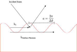
Nevertheless, coupling of photons into SPPs can be achieved using a coupling medium such as a prism or grating to match the photon and surface plasmon wave vectors. A prism can be positioned against a thin metal film in the Kretschmann configuration or very close to a metal surface in the Otto configuration (Figure 1). A grating coupler matches the wave vectors by increasing the parallel wave vector component by an amount related to the grating period (Figure 2). This method, while less frequently utilized, is critical to the theoretical understanding of the effect of surface roughness. Moreover, simple isolated surface defects such as a groove, a slit or a corrugation on an otherwise planar surface provides a mechanism by which free-space radiation and SPs can exchange energy and hence couple.
Dispersion relation
The electric field of a propagating electromagnetic wave can be expressed
![E= E_{0}\exp[i(k_{x} x + k_{z} z -\omega t)]\,](../I/m/b80fd5c7853aed0445052ac3bc28c8dc.png)
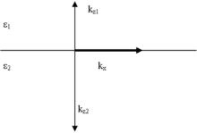
where k is the wave number and ω is the frequency of the wave. By solving Maxwell's equations for the electromagnetic wave at an interface between two materials with relative dielectric functions ε1 and ε2 (see figure 3) with the appropriate continuity relation the boundary conditions are[7][8]
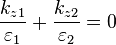
and
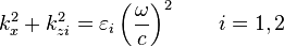
where c is the speed of light in a vacuum, and kx is same for both media at the interface for a surface wave. Solving these two equations, the dispersion relation for a wave propagating on the surface is
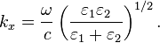
In the free electron model of an electron gas, which neglects attenuation, the metallic dielectric function is[9]
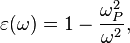
where the bulk plasma frequency in SI units is
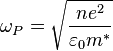
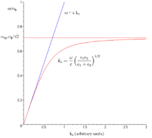
where n is the electron density, e is the charge of the electron, m* is the effective mass of the electron and  is the permittivity of free-space. The dispersion relation is plotted in Figure 4. At low k, the SPP behaves like a photon, but as k increases, the dispersion relation bends over and reaches an asymptotic limit called the "surface plasma frequency". Since the dispersion curve lies to the right of the light line, ω = k·c, the SPP has a shorter wavelength than free-space radiation such that the out-of-plane component of the SPP wavevector is purely imaginary and exhibits evanescent decay. The surface plasma frequency is the asymptote of this curve, and is given by

In the case of air, this result simplifies to

If we assume that ε2 is real and ε2 > 0, then it must be true that ε1 < 0, a condition which is satisfied in metals. Electromagnetic waves passing through a metal experience damping due to Ohmic losses and electron-core interactions. These effects show up in as an imaginary component of the dielectric function. The dielectric function of a metal is expressed ε1 = ε1' + i·ε1" where ε1' and ε1" are the real and imaginary parts of the dielectric function, respectively. Generally |ε1'| >> ε1" so the wavenumber can be expressed in terms of its real and imaginary components as[7]
![k_{x}=k_{x}'+i k_{x}''=\left[\frac{\omega}{c} \left( \frac{\varepsilon_1' \varepsilon_2}{\varepsilon_1' + \varepsilon_2}\right)^{1/2}\right] + i \left[\frac{\omega}{c} \left( \frac{\varepsilon_1' \varepsilon_2}{\varepsilon_1' + \varepsilon_2}\right)^{3/2} \frac{\varepsilon_1''}{2(\varepsilon_1')^2}\right].](../I/m/806548d4a83b85b84be5d3aca3dc678f.png)
The wave vector gives us insight into physically meaningful properties of the electromagnetic wave such as its spatial extent and coupling requirements for wave vector matching.
Propagation length and skin depth
As an SPP propagates along the surface, it loses energy to the metal due to absorption. The intensity of the surface plasmon decays with the square of the electric field, so at a distance x, the intensity has decreased by a factor of exp[-2kx"x]. The propagation length is defined as the distance for the SPP intensity to decay by a factor of 1/e. This condition is satisfied at a length[10]

Likewise, the electric field falls off evanescently perpendicular to the metal surface. At low frequencies, the SPP penetration depth into the metal is commonly approximated using the skin depth formula. In the dielectric, the field will fall off far more slowly. The decay lengths in the metal and dielectric medium can be expressed as[10]
where i indicates the medium of propagation. SPPs are very sensitive to slight perturbations within the skin depth and because of this, SPPs are often used to probe inhomogeneities of a surface.
Animations
-
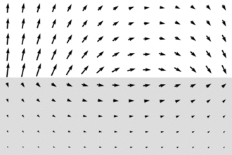
The electric field (E-field) of an SPP at the silver-air interface, at the frequency where the free-space wavelength is 370 nm. The animation shows how the E-field varies over an optical cycle. The permittivity of silver at this frequency is (-2.6 + 0.6i). The picture is (0.3 × 370nm) across horizontally; the SPP wavelength is much smaller than the free-space wavelength.
-
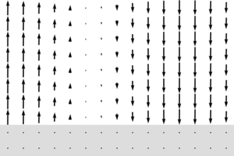
The E-field of an SPP at the silver-air interface, at a much lower frequency corresponding to a free-space wavelength of 10μm. At this frequency, the silver behaves approximately as a perfect electric conductor, and the SPP is called a Sommerfeld Zenneck wave, with almost the same wavelength as the free-space wavelength. The permittivity of silver at this frequency is (-2700 + 1400i). The picture is (0.6 × 10μm) across horizontally.
Experimental applications
Nanofabricated systems that exploit SPPs demonstrate potential for designing and controlling the propagation of light in matter. In particular, SPPs can be used to channel light efficiently into nanometer scale volumes, leading to direct modification of resonate frequency dispersion properties (substantially shrinking the wavelength of light and the speed of light pulses for example), as well as field enhancements suitable for enabling strong interactions with nonlinear materials. The resulting enhanced sensitivity of light to external parameters (for example, an applied electric field or the dielectric constant of an adsorbed molecular layer) shows great promise for applications in sensing and switching.
Current research is focused on the design, fabrication, and experimental characterization of novel components for measurement and communications based on nanoscale plasmonic effects. These devices include ultra-compact plasmonic interferometers for applications such as biosensing, optical positioning and optical switching, as well as the individual building blocks (plasmon source, waveguide and detector) needed to integrate a high-bandwidth, infrared-frequency plasmonic communications link on a silicon chip.
In addition to building functional devices based on SPPs, it appears feasible to exploit the dispersion characteristics of SPPs traveling in confined metallo-dielectric spaces to create photonic materials with artificially tailored bulk optical characteristics, otherwise known as metamaterials.[5]
The excitation of SPPs is frequently used in an experimental technique known as surface plasmon resonance (SPR). In SPR, the maximum excitation of surface plasmons are detected by monitoring the reflected power from a prism coupler as a function of incident angle or wavelength. This technique can be used to observe nanometer changes in thickness, density fluctuations, or molecular absorption.
Surface plasmon-based circuits, including both SPPs and localized plasmon resonances, have been proposed as a means of overcoming the size limitations of photonic circuits for use in high performance data processing nano devices.[11]
The ability to dynamically control the plasmonic properties of materials in these nano-devices is key to their development. A new approach that uses plasmon-plasmon interactions has been demonstrated recently. Here the bulk plasmon resonance is induced or suppressed to manipulate the propagation of light.[12] This approach has been shown to have a high potential for nanoscale light manipulation and the development of a fully CMOS- compatible electro-optical plasmonic modulator.
CMOS compatible electro-optic plasmonic modulators will be key components in chip-scale photonic circuits.[13]
In surface second harmonic generation, the second harmonic signal is proportional to the square of the electric field. The electric field is stronger at the interface because of the surface plasmon resulting in a non-linear optical effect. This larger signal is often exploited to produce a stronger second harmonic signal.[14]
The wavelength and intensity of the plasmon-related absorption and emission peaks are affected by molecular adsorption that can be used in molecular sensors. For example, a fully operational prototype device detecting casein in milk has been fabricated. The device is based on monitoring changes in plasmon-related absorption of light by a gold layer.[15]
Effects of roughness
In order to understand the effect of roughness on SPPs, it is beneficial to first understand how a SPP is coupled by a grating Figure2. When a photon is incident on a surface, the wave vector of the photon in the dielectric material is smaller than that of the SPP. In order for the photon to couple into a SPP, the wave vector must increase by  . The grating harmonics of a periodic grating provide additional momentum parallel to the supporting interface to match the terms.

where  is the wave vector of the grating,
  is the angle of incidence of the incoming photon, a is the grating period, and n is an integer.
Rough surfaces can be thought of as the superposition of many gratings of different periodicities. Kretschmann proposed[16] that a statistical correlation function be defined for a rough surface
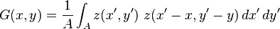
where  is the height above the mean surface height at the position
  , and
, and  is the area of integration. Assuming that the statistical correlation function is Gaussian of the form
where  is the root mean square height,
  is the distance from the point , and
  is the correlation length, then the Fourier transform of the correlation function is
where  is a measure of the amount of each spatial frequency
  which help couple photons into a surface plasmon.
If the surface only has one Fourier component of roughness (i.e. the surface profile is sinusoidal), then the is discrete and exists only at  , resulting in a single narrow set of angles for coupling. If the surface contains many Fourier components, then coupling becomes possible at multiple angles. For a random surface, becomes continuous and the range of coupling angles broadens.
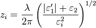
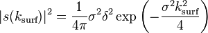
As stated earlier, SPPs are non-radiative. When a SPP travels along a rough surface, it usually becomes radiative due to scattering. The Surface Scattering Theory of light suggests that the scattered intensity  per solid angle
  per incident intensity
  is[17]
where  is the radiation pattern from a single dipole at the metal/dielectric interface. If surface plasmons are excited in the Kretschmann geometry and the scattered light is observed in the plane of incidence (Fig. 4), then the dipole function becomes
![|W|^2=A(\theta,|\varepsilon_{1}|)\ \sin^2{\psi} \ [(1+\sin^2 \theta /|\varepsilon_1|)^{1/2} - \sin{\theta}]^2](../I/m/b727f993c57727e22a639c73127fec30.png)
with

where  is the polarization angle and
  is the angle from the z-axis in the xz-plane. Two important consequences come out of these equations. The first is that if
  (s-polarization), then
  and the scattered light
  . Secondly, the scattered light has a measurable profile which is readily correlated to the roughness. This topic is treated in greater detail in reference.[17]
See also
References
- ↑ S.Zeng; Baillargeat, Dominique; Ho, Ho-Pui; Yong, Ken-Tye et al. (2014). "Nanomaterials enhanced surface plasmon resonance for biological and chemical sensing applications". Chemical Society Reviews 43 (10): 3426–3452. doi:10.1039/C3CS60479A. PMID 24549396.
- ↑ 2.0 2.1 2.2 NIST researchers, Nanofabrication Research Group. "Three-Dimensional Plasmonic Metamaterials". National Institute of Science and Technology. Retrieved 2011-02-15.
- NIST researchers, Nanofabrication Research Group. "Opto-mechanical Devices for Measuring Nanoplasmonic Metamaterials". National Institute of Science and Technology. Retrieved 2011-02-15.
 This article incorporates public domain material from the National Institute of Standards and Technology document "Three-Dimensional Plasmonic Metamaterials".
- ↑ Yarris, Lynn. "GRIN Plasmonics..." (Online news release). U.S. Department of Energy National Laboratory Operated by the University of California. Retrieved 2011-02-15.
- ↑ Barnes, William L.; Dereux, Alain; Ebbesen, Thomas W. (2003). "Surface plasmon subwavelength optics". Nature 424 (6950): 824–30. Bibcode:2003Natur.424..824B. doi:10.1038/nature01937. PMID 12917696.
- Huidobro, Paloma A.; Nesterov, Maxim L.; Martín-Moreno, Luis; García-Vidal, Francisco J. (2010). "Transformation Optics for Plasmonics". Nano Letters 10 (6): 1985–90. arXiv:1003.1154. Bibcode:2010NanoL..10.1985H. doi:10.1021/nl100800c. PMID 20465271. Free PDF download for these peer reviewed articles.
- PDF from arxiv.org - Transformation Optics for Plasmonics. 15 pages.
- ↑ 5.0 5.1 NIST researchers, Nanofabrication Research Group. "Nanoplasmonics" (Online). National Institute of Science and Technology. Retrieved 2011-02-15.
- This article incorporates public domain material from the National Institute of Standards and Technology document "Nanoplasmonics".
- ↑ Zeng, Shuwen; Yu, Xia; Law, Wing-Cheung; Zhang, Yating; Hu, Rui; Dinh, Xuan-Quyen; Ho, Ho-Pui; Yong, Ken-Tye (2013). "Size dependence of Au NP-enhanced surface plasmon resonance based on differential phase measurement". Sensors and Actuators B: Chemical 176: 1128. doi:10.1016/j.snb.2012.09.073.
- ↑ 7.0 7.1 Raether, Heinz (1988). Surface Plasmons on Smooth and Rough Surfaces and on Gratings. Springer Tracts in Modern Physics 111. New York: Springer-Verlag. ISBN 3540173633.
- ↑ Cottam, Michael G. (1989). Introduction to Surface and Superlattice Excitations. New York: Cambridge University Press. ISBN 0750305886.
- ↑ Kittel, Charles (1996). Introduction to Solid State Physics (8th ed.). Hoboken, NJ: John Wiley & Sons. ISBN 0-471-41526-X.
- ↑ 10.0 10.1 Homola, Jirí (2006). Surface Plasmon Resonance Based Sensors. Springer Series on Chemical Sensors and Biosensors, 4. Berlin: Springer-Verlag. ISBN 3-540-33918-3.
- ↑ Ozbay, E. (2006). "Plasmonics: Merging Photonics and Electronics at Nanoscale Dimensions". Science 311 (5758): 189–93. Bibcode:2006Sci...311..189O. doi:10.1126/science.1114849. PMID 16410515.
- ↑ Akimov, Yu A; Chu, H S (2012). "Plasmon–plasmon interaction: Controlling light at nanoscale". Nanotechnology 23 (44): 444004. doi:10.1088/0957-4484/23/44/444004. PMID 23080049.
- ↑ Wenshan Cai, Justin S. White, and Mark L. Brongersma (2009). "Compact, High-Speed and Power-Efficient Electrooptic Plasmonic Modulators". Nano Letters 9 (12): 4403–11. Bibcode:2009NanoL...9.4403C. doi:10.1021/nl902701b. PMID 19827771.
- ↑ V. K. Valev (2012). "Characterization of Nanostructured Plasmonic Surfaces with Second Harmonic Generation". Langmuir 28 (44): 15454–15471. doi:10.1021/la302485c.
- ↑ Minh Hiep, Ha; Endo, Tatsuro; Kerman, Kagan; Chikae, Miyuki; Kim, Do-Kyun; Yamamura, Shohei; Takamura, Yuzuru; Tamiya, Eiichi (2007). "A localized surface plasmon resonance based immunosensor for the detection of casein in milk". Science and Technology of Advanced Materials (free download pdf) 8 (4): 331. Bibcode:2007STAdM...8..331M. doi:10.1016/j.stam.2006.12.010.
- ↑ Kretschmann, E. (April 1974). "Die Bestimmung der Oberflächenrauhigkeit dünner Schichten durch Messung der Winkelabhängigkeit der Streustrahlung von Oberflächenplasmaschwingungen". Optics Communications (in German) 10 (4): 353–356. Bibcode:1974OptCo..10..353K. doi:10.1016/0030-4018(74)90362-9.
- ↑ 17.0 17.1 Kretschmann, E. (1972). "The angular dependence and the polarisation of light emitted by surface plasmons on metals due to roughness". Optics Communications 5 (5): 331–336. Bibcode:1972OptCo...5..331K. doi:10.1016/0030-4018(72)90026-0.
Further reading
- Ebbesen, T. W.; Lezec, H. J.; Ghaemi, H. F.; Thio, T.; Wolff, P. A. (1998). "Extraordinary optical transmission through sub-wavelength hole arrays". Nature 391 (6668): 667. Bibcode:1998Natur.391..667E. doi:10.1038/35570.
- Hendry, E.; Garcia-Vidal, F.; Martin-Moreno, L.; Rivas, J.; Bonn, M.; Hibbins, A.; Lockyear, M. (2008). "Optical Control over Surface-Plasmon-Polariton-Assisted THz Transmission through a Slit Aperture". Physical Review Letters 100 (12): 123901. Bibcode:2008PhRvL.100l3901H. doi:10.1103/PhysRevLett.100.123901. PMID 18517865. Free PDF download.
- Barnes, William L.; Dereux, Alain; Ebbesen, Thomas W. (2003). "Surface plasmon subwavelength optics". Nature 424 (6950): 824–30. Bibcode:2003Natur.424..824B. doi:10.1038/nature01937. PMID 12917696. Free PDF download.
- Pitarke, J M; Silkin, V M; Chulkov, E V; Echenique, P M (2007). "Theory of surface plasmons and surface-plasmon polaritons". Reports on Progress in Physics 70: 1. arXiv:cond-mat/0611257. Bibcode:2007RPPh...70....1P. doi:10.1088/0034-4885/70/1/R01. Free PDF download.
External links
- White, Justin (March 19, 2007). "Surface Plasmon Polaritons" (Online). Stanford University. Physics department. "Submitted as coursework for AP272. Winter 2007".