Surface plasmon

Surface plasmons (SPs) are coherent delocalized electron oscillations that exist at the interface between any two materials where the real part of the dielectric function changes sign across the interface (e.g. a metal-dielectric interface, such as a metal sheet in air). SPs have lower energy than bulk (or volume) plasmons which quantise the longitudinal electron oscillations about positive ion cores within the bulk of an electron gas (or plasma).
The charge motion in a surface plasmon always creates electromagnetic fields outside (as well as inside) the metal. The total excitation, including both the charge motion and associated electromagnetic field, is called either a surface plasmon polariton at a planar interface, or a localized surface plasmon for the closed surface of a small particle.
The existence of surface plasmons was first predicted in 1957 by Rufus Ritchie.[1] In the following two decades, surface plasmons were extensively studied by many scientists, the foremost of whom were T. Turbadar in the 1950s and 1960s, and Heinz Raether, E. Kretschmann, and A. Otto in the 1960s and 1970s. Information transfer in nanoscale structures, similar to photonics, by means of surface plasmons, is referred to as plasmonics.[2]
Surface plasmon polaritons
Excitation
Surface plasmon polaritons can be excited by electrons or photons. In the case of photons, it cannot be done directly, but requires a prism, or a grating, or a defect on the metal surface.
Dispersion relation

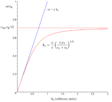
At low frequency, an SPP approaches a Sommerfeld-Zenneck wave, where the dispersion relation (relation between frequency and wavevector) is the same as in free space. At high frequency, the dispersion relation bends over and reaches an asymptotic limit called the "surface plasma frequency". (See figure at right.) For more details see surface plasmon polariton.
Propagation length and skin depth
| Condensed matter physics |
|---|
 |
| Phases · Phase transition |
|
Solid · Liquid · Gas · Plasma · Bose–Einstein condensate · Bose gas · Fermionic condensate · Fermi gas · Fermi liquid · Supersolid · Superfluidity · Luttinger liquid |
|
Phase phenomena |
|
Electronic phases Electronic band structure · Insulator · Mott insulator · Semiconductor · Semimetal · Conductor · Superconductor · Thermoelectric · Piezoelectric · Ferroelectric · topological insulator |
|
Electronic phenomena |
|
Magnetic phases |
|
Scientists Van der Waals · Onnes · von Laue · Bragg · Debye · Bloch · Onsager · Mott · Peierls · Landau · Luttinger · Anderson · Van Vleck · Mott · Hubbard · Shockley · Bardeen · Cooper · Schrieffer · Josephson · Louis Néel · Esaki · Giaever · Kohn · Kadanoff · Fisher · Wilson · von Klitzing · Binnig · Rohrer · Bednorz · Müller · Laughlin · Störmer · Tsui · Abrikosov · Ginzburg · Leggett |
As an SPP propagates along the surface, it loses energy to the metal due to absorption. It can also lose energy due to scattering into free-space or into other directions. The electric field falls off evanescently perpendicular to the metal surface. At low frequencies, the SPP penetration depth into the metal is commonly approximated using the skin depth formula. In the dielectric, the field will fall off far more slowly. SPPs are very sensitive to slight perturbations within the skin depth and because of this, SPPs are often used to probe inhomogeneities of a surface. For more details see surface plasmon polariton.
Experimental applications
The excitation of surface plasmons is frequently used in an experimental technique known as surface plasmon resonance (SPR). In SPR, the maximum excitation of surface plasmons are detected by monitoring the reflected power from a prism coupler as a function of incident angle or wavelength. This technique can be used to observe nanometer changes in thickness, density fluctuations, or molecular absorption.

Surface plasmon-based circuits have been proposed as a means of overcoming the size limitations of photonic circuits for use in high performance data processing nano devices.[4]
The ability to dynamically control the plasmonic properties of materials in these nano-devices is key to their development. A new approach that uses plasmon-plasmon interactions has been demonstrated recently. Here the bulk plasmon resonance is induced or suppressed to manipulate the propagation of light.[5] This approach has been shown to have a high potential for nanoscale light manipulation and the development of a fully CMOS- compatible electro-optical plasmonic modulator, said to be a future key component in chip-scale photonic circuits.[6]
In surface second harmonic generation, the second harmonic signal is proportional to the square of the electric field. The electric field is stronger at the interface because of the surface plasmon resulting in a non-linear optical effect. This larger signal is often exploited to produce a stronger second harmonic signal.[7]
The wavelength and intensity of the plasmon-related absorption and emission peaks are affected by molecular adsorption that can be used in molecular sensors. For example, a fully operational prototype device detecting casein in milk has been fabricated. The device is based on monitoring changes in plasmon-related absorption of light by a gold layer.[8]
See also
- Localized surface plasmon
- Waves in plasmas
- Free electron model
- Plasma oscillation
- Biosensor
- Spinplasmonics
- extraordinary optical transmission
- Dual-polarization interferometry
- Plasmonic lens
- List of plasma (physics) articles
References
- ↑ Ritchie, R. H. (June 1957). "Plasma Losses by Fast Electrons in Thin Films". Physical Review 106 (5): 874–881. Bibcode:1957PhRv..106..874R. doi:10.1103/PhysRev.106.874.
- ↑ Polman, Albert; Harry A. Atwater (2005). "Plasmonics: optics at the nanoscale". Materials Today. 8 (2005): 56. doi:10.1016/S1369-7021(04)00685-6. Retrieved January 26, 2011.
- ↑ S.Zeng; Baillargeat, Dominique; Ho, Ho-Pui; Yong, Ken-Tye et al. (2014). "Nanomaterials enhanced surface plasmon resonance for biological and chemical sensing applications". Chemical Society Reviews 43 (10): 3426–3452. doi:10.1039/C3CS60479A. PMID 24549396.
- ↑ Ozbay, E. (2006). "Plasmonics: Merging Photonics and Electronics at Nanoscale Dimensions". Science 311 (5758): 189–93. Bibcode:2006Sci...311..189O. doi:10.1126/science.1114849. PMID 16410515.
- ↑ Akimov, Yu A; Chu, H S (2012). "Plasmon–plasmon interaction: Controlling light at nanoscale". Nanotechnology 23 (44): 444004. doi:10.1088/0957-4484/23/44/444004. PMID 23080049.
- ↑ Wenshan Cai, Justin S. White, and Mark L. Brongersma (2009). "Compact, High-Speed and Power-Efficient Electrooptic Plasmonic Modulators". Nano Letters 9 (12): 4403–11. Bibcode:2009NanoL...9.4403C. doi:10.1021/nl902701b. PMID 19827771.
- ↑ V. K. Valev (2012). "Characterization of Nanostructured Plasmonic Surfaces with Second Harmonic Generation". Langmuir 28 (44): 15454–15471. doi:10.1021/la302485c.
- ↑ Minh Hiep, Ha; Endo, Tatsuro; Kerman, Kagan; Chikae, Miyuki; Kim, Do-Kyun; Yamamura, Shohei; Takamura, Yuzuru; Tamiya, Eiichi (2007). "A localized surface plasmon resonance based immunosensor for the detection of casein in milk". Science and Technology of Advanced Materials (free download pdf) 8 (4): 331. Bibcode:2007STAdM...8..331M. doi:10.1016/j.stam.2006.12.010.