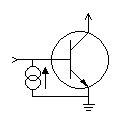
Integrated injection logic

Integrated injection logic (IIL, I2L, or I2L) is a class of digital circuits built with multiple collector bipolar junction transistors (BJT).[1] When introduced it had speed comparable to TTL yet was almost as low power as CMOS, making it ideal for use in VLSI (and larger) integrated circuits. Although the logic voltage levels are very close (High: 0.7V, Low: 0.2V), I2L has high noise immunity because it operates by current instead of voltage. It is sometimes also known as merged transistor logic.
Operation

The heart of an I2L circuit is the common emitter open collector inverter. Typically, an inverter consists of an NPN transistor with the emitter connected to ground and the base biased with a forward current. The input is supplied to the base as either a current sink (low logic level) or as a high-z floating condition (high logic level). The output of an inverter is at the collector. Likewise, it is either a current sink (low logic level) or a high-z floating condition (high logic level).
Like direct-coupled transistor logic, there is no resistor between the output (collector) of one NPN transistor and the input (base) of the following transistor.
To understand how the inverter operates, it is necessary to understand the current flow. If the bias current is shunted to ground (low logic level), the transistor turns off and the collector floats (high logic level). If the bias current is not shunted to ground because the input is high-z (high logic level), the bias current flows through the transistor to the emitter, switching on the transistor, and allowing the collector to sink current (low logic level). Because the output of the inverter can sink current but cannot source current, it is safe to connect the outputs of multiple inverters together to form a wired AND gate. When the outputs of two inverters are wired together, the result is a two-input NOR gate because the configuration (NOT A) AND (NOT B) is equivalent to NOT (A OR B) (per De Morgan's Theorem).
Usage
I2L is relatively simple to construct on an integrated circuit, and was commonly used before the advent of CMOS logic by companies such as Motorola (now Freescale)[2] and Texas Instruments. In 1975, Sinclair Radionics introduced one of the first consumer-grade digital watches, the Black Watch, which used I2L technology.[3] In 1979, HP introduced a frequency measurement instrument based on a HP-made custom LSI chip that uses integrated injection logic (I2L) for low power consumption and high density, enabling portable battery operation, and also some emitter function logic (EFL) circuits where high speed is needed.[4]
Generally, I2L gates were constructed with transistors with 1, 2 or 3 separate collectors. This fan-out of up to 3 allowed 3-input NAND or NOR gates to be constructed very simply with just a single layer of interconnect metal.
RCA used I²L in late 1970s in its CA3162 ADC 3 digit meter.
References
- ↑ Hart, K.; Slob, A. (Oct 1972). "Integrated Injection Logic: A New Approach to LSI". IEEE Journal of Solid-State Circuits 7 (5): 346–351. doi:10.1109/jssc.1972.1052891.
- ↑ Jarrett, Robert. "A monolithic speed-control micro-system for automotive applications". IEEE.ORG. IEEE. Retrieved 21 June 2014.
- ↑ "Clive Sinclair's 1982 Practical Computing Interview". Retrieved 21 June 2014.
- ↑ "HP memory project: Time, Frequency Standard & Counter"
| ||||||||||