Integrated circuit packaging

In electronics manufacturing, integrated circuit packaging is the final stage of semiconductor device fabrication, in which the tiny block of semiconducting material is encased in a supporting case that prevents physical damage and corrosion. The case, known as a "package", supports the electrical contacts which connect the device to a circuit board.
In the integrated circuit industry it is called simply packaging and sometimes semiconductor device assembly, or simply assembly. Sometimes it is called encapsulation or seal. The packaging stage is followed by testing of the integrated circuit.
The term is sometimes confused with electronic packaging, which is the mounting and interconnecting of integrated circuits (and other components) onto printed-circuit boards.
Approaches
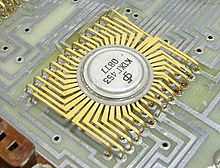
The earliest integrated circuits were packaged in ceramic flat packs, which the military used for many years for their reliability and small size. Commercial circuit packaging quickly moved to the dual in-line package (DIP), first in ceramic and later in plastic. In the 1980s VLSI pin counts exceeded the practical limit for DIP packaging, leading to pin grid array (PGA) and leadless chip carrier (LCC) packages. Surface mount packaging appeared in the early 1980s and became popular in the late 1980s, using finer lead pitch with leads formed as either gull-wing or J-lead, as exemplified by small-outline integrated circuit — a carrier which occupies an area about 30 – 50% less than an equivalent DIP, with a typical thickness that is 70% less. This package has "gull wing" leads protruding from the two long sides and a lead spacing of 0.050 inches.
An area array package places the interconnection terminals on the surface area, providing a greater number of connections than where only the outer perimeter is used. The first chip package of this kind was a ceramic pin grid array.[1] The plastic ball grid array is the most commonly used.[2]
In the late 1990s, plastic quad flat pack(PQFP) and thin small-outline packages (TSOP) became the most common for high pin count devices, though PGA packages are still often used for microprocessors. Intel and AMD transitioned in the 2000s from PGA packages to land grid array (LGA) packages.
Ball grid array (BGA) packages have existed since the 1970s. Flip-chip ball grid array packages (FCBGA) developed in the 1990s allow for much higher pin count than other package types. In an FCBGA package the die is mounted upside-down (flipped) and connects to the package balls via a substrate that is similar to a printed-circuit board rather than by wires. FCBGA packages allow an array of input-output signals (called Area-I/O) to be distributed over the entire die rather than being confined to the die periphery.
Traces out of the die, through the package, and into the printed circuit board have very different electrical properties, compared to on-chip signals. They require special design techniques and need much more electric power than signals confined to the chip itself.
Stacking multiple dies in one package is called SiP, for System In Package, or three-dimensional integrated circuit. Combining multiple dies on a small substrate, often ceramic, is called an MCM, or Multi-Chip Module. The boundary between a big MCM and a small printed circuit board is sometimes blurry.
Operations
The following operations are performed at the stage of packaging.
Die attachment is the step during which a die is mounted and fixed to the package or support structure (header).[3] For high-powered applications, the die is usually eutectic bonded onto the package, using e.g. gold-tin or gold-silicon solder (for good heat conduction). For low-cost, low-powered applications, the die is often glued directly onto a substrate (such as a printed wiring board) using an epoxy adhesive.
- IC Bonding
- Wire bonding
- Thermosonic Bonding
- Down bonding
- Tape-automated bonding
- Flip chip
- Quilt packaging
- Tab bonding
- Film attaching
- Spacer attaching
- IC encapsulation
- Wafer bonding
See also
- List of integrated circuit packaging types
- List of electronics package dimensions
- B-staging
- Potting (electronics)
- Quilt packaging
- Electronic packaging
- Chip carrier category
References
- ↑ William J. Greig (2007). Integrated circuit packaging, assembly and interconnections. Springer. pp. 36–41. ISBN 0-387-28153-3.
- ↑ Ken Gilleo (2003). Area array packaging processes for BGA, Flip Chip, and CSP. McGraw-Hill Professional. p. 251. ISBN 0-07-142829-1.
- ↑ L. W. Turner (ed), Electronics Engineers Reference Book, Newnes-Butterworth, 1976, ISBN 0-408-00168-2, pages 11-34 through 11-37
External links
- ivf.se – The Nordic Electronics Packaging Guideline Investigation on the technical performance of different packaging and interconnection systems
| ||||||||||||||||||||||||||||||||||||||