Hybrid-pi model
The hybrid-pi model is a popular circuit model used for analyzing the small signal behavior of bipolar junction and field effect transistors. Sometimes it is also called "Giacoletto model" because it was introduced by L.J. Giacoletto in 1969.[1] The model can be quite accurate for low-frequency circuits and can easily be adapted for higher frequency circuits with the addition of appropriate inter-electrode capacitances and other parasitic elements.
Bipolar junction (BJT) parameters
The hybrid-pi model is a linearized two-port network approximation to the BJT using the small-signal base-emitter voltage  and collector-emitter voltage
  as independent variables, and the small-signal base current
  and collector current
  as dependent variables.[2]

A basic, low-frequency hybrid-pi model for the bipolar transistor is shown in figure 1. The various parameters are as follows.
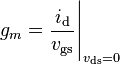
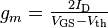
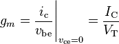 is the transconductance in siemens, evaluated in a simple model[3]
- where:
-
 is the quiescent collector current (also called the collector bias or DC collector current)
 -
 is the thermal voltage, calculated from Boltzmann's constant
  , the charge of an electron
  , and the transistor temperature in kelvins,
  . At approximately room temperature (295K, 22°C or 71°F)
  is about 25 mV.
-
-
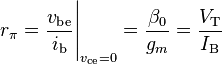 in ohms
- where:
-
 is the current gain at low frequencies (commonly called hFE). Here
  is the DC (bias) base current. This is a parameter specific to each transistor, and can be found on a datasheet.
-
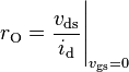
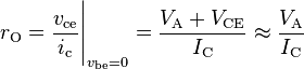 is the output resistance due to the Early effect (
 is the Early voltage).
Related terms
The reciprocal of the output resistance is named the output conductance
 .
.
The reciprocal of gm is called the intrinsic resistance
 .
.
Full model
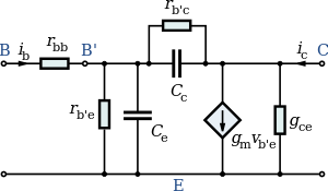
The full model introduces the virtual terminal B' so that the base spreading resistance rbb (the bulk resistance between the base contact and the active region of the base under the emitter) and rb'e (representing the base current required to make up for recombination of minority carriers in the base region) can be represented separately. Ce is the diffusion capacitance representing minority carrier storage in the base. The feedback components rb'c and Cc are introduced to represent the Early effect.[4]
MOSFET parameters

A basic, low-frequency hybrid-pi model for the MOSFET is shown in figure 2. The various parameters are as follows.
is the transconductance in siemens, evaluated in the Shichman-Hodges model in terms of the Q-point drain current  by (see Jaeger and Blalock[5]):
 ,
,
- where:
- is the quiescent drain current (also called the drain bias or DC drain current)
 = threshold voltage and
  = gate-to-source voltage.
The combination:

is often called overdrive voltage.
 is the output resistance due to channel length modulation, calculated using the Shichman-Hodges model as
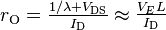 ,
,
using the approximation for the channel length modulation parameter λ[6]
 .
.
Here VE is a technology-related parameter (about 4 V/μm for the 65 nm technology node[6]) and L is the length of the source-to-drain separation.
The reciprocal of the output resistance is named the drain conductance
 .
.
See also
- Small signal model
- h-parameter model
References and notes
- ↑ Giacoletto, L.J. "Diode and transistor equivalent circuits for transient operation" IEEE Journal of Solid-State Circuits, Vol 4, Issue 2, 1969
- ↑ R.C. Jaeger and T.N. Blalock (2004). Microelectronic Circuit Design (Second Edition ed.). New York: McGraw-Hill. pp. Section 13.5, esp. Eqs. 13.19. ISBN 0-07-232099-0.
- ↑ R.C. Jaeger and T.N. Blalock. Eq. 5.45 pp. 242 and Eq. 13.25 p. 682. ISBN 0-07-232099-0.
- ↑ Dhaarma Raj Cheruku, Battula Tirumala Krishna, Electronic Devices And Circuits, pages 281-282, Pearson Education India, 2008 ISBN 8131700984.
- ↑ R.C. Jaeger and T.N. Blalock. Eq. 4.20 pp. 155 and Eq. 13.74 p. 702. ISBN 0-07-232099-0.
- ↑ 6.0 6.1 W. M. C. Sansen (2006). Analog Design Essentials. Dordrechtμ: Springer. p. §0124, p. 13. ISBN 0-387-25746-2.