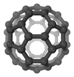
Graphene

Graphene (/ˈɡræf.iːn/)[1][2] is an allotrope of carbon in the form of a two-dimensional, atomic-scale, hexagonal lattice in which one atom forms each vertex. It is the basic structural element of other allotropes, including graphite, charcoal, carbon nanotubes and fullerenes. It can also be considered as an indefinitely large aromatic molecule, the limiting case of the family of flat polycyclic aromatic hydrocarbons.

Graphene has many extraordinary properties. It is about 100 times stronger than steel by weight,[3] conducts heat and electricity with great efficiency and is nearly transparent.[4] Researchers have identified the bipolar transistor effect, ballistic transport of charges and large quantum oscillations in the material.
Scientists have theorized about graphene for decades. It is quite likely that graphene was unwittingly produced in small quantities for centuries through the use of pencils and other similar applications of graphite, but it was first measurably produced and isolated in the lab in 2003.[5] Research was informed by existing theoretical descriptions of its composition, structure and properties.[6] High-quality graphene proved to be surprisingly easy to isolate, making more research possible.
Andre Geim and Konstantin Novoselov at the University of Manchester won the Nobel Prize in Physics in 2010 "for groundbreaking experiments regarding the two-dimensional material graphene."[7]
The global market for graphene is reported to have reached $9 million by 2014 with most sales in the semiconductor, electronics, battery energy and composites industries.[8]
Definition
"Graphene" is a combination of graphite and the suffix -ene, named by Hanns-Peter Boehm,[9] who described single-layer carbon foils in 1962.[10]
The term graphene first appeared in 1987[11] to describe single sheets of graphite as a constituent of graphite intercalation compounds (GICs); conceptually a GIC is a crystalline salt of the intercalant and graphene. The term was also used in early descriptions of carbon nanotubes,[12] as well as for epitaxial graphene[13] and polycyclic aromatic hydrocarbons.[14] Graphene can be considered an "infinite alternant" (only six-member carbon ring) polycyclic aromatic hydrocarbon (PAH).[15]
The IUPAC compendium of technology states: "previously, descriptions such as graphite layers, carbon layers, or carbon sheets have been used for the term graphene... it is incorrect to use for a single layer a term which includes the term graphite, which would imply a three-dimensional structure. The term graphene should be used only when the reactions, structural relations or other properties of individual layers are discussed."[16]
Geim defined "isolated or free-standing graphene" as "graphene is a single atomic plane of graphite, which – and this is essential – is sufficiently isolated from its environment to be considered free-standing."[17] This definition is narrower than the IUPAC definition and refers to cloven, transferred, and suspended graphene. Other forms of graphene, such as graphene grown on various metals, can become free-standing if, for example, suspended or transferred to silicon dioxide (SiO
2) or silicon carbide.[18]
History
In 1859 Benjamin Collins Brodie was aware of the highly lamellar structure of thermally reduced graphite oxide.[19][20]
The structure of graphite was solved in 1916[21] by the related method of powder diffraction.[22] It was studied in detail by V. Kohlschütter and P. Haenni in 1918, who also described the properties of graphite oxide paper.[23] Its structure was determined from single-crystal diffraction in 1924.[24]
The theory of graphene was first explored by P. R. Wallace in 1947 as a starting point for understanding the electronic properties of 3D graphite. The emergent massless Dirac equation was first pointed out by Gordon Walter Semenoff and David P. DeVincenzo and Eugene J. Mele.[25] Semenoff emphasized the occurrence in a magnetic field of an electronic Landau level precisely at the Dirac point. This level is responsible for the anomalous integer quantum Hall effect.[26][27][28]
The earliest TEM images of few-layer graphite were published by G. Ruess and F. Vogt in 1948.[29] Later, single graphene layers were also observed directly by electron microscopy.[30] Before 2004 intercalated graphite compounds were studied under a transmission electron microscope (TEM). Researchers occasionally observed thin graphitic flakes ("few-layer graphene") and possibly even individual layers. An early, detailed study on few-layer graphite dates to 1962.[31][32]
Starting in the 1970s single layers of graphite were grown epitaxially on top of other materials.[33] This "epitaxial graphene" consists of a single-atom-thick hexagonal lattice of sp2-bonded carbon atoms, as in free-standing graphene. However, there is significant charge transfer from the substrate to the epitaxial graphene, and, in some cases, hybridization between the d-orbitals of the substrate atoms and π orbitals of graphene, which significantly alters the electronic structure of epitaxial graphene.
Single layers of graphite were also observed by transmission electron microscopy within bulk materials, in particular inside soot obtained by chemical exfoliation. Efforts to make thin films of graphite by mechanical exfoliation started in 1990,[34] but nothing thinner than 50 to 100 layers was produced before 2004.

Initial attempts to make atomically thin graphitic films employed exfoliation techniques similar to the drawing method. Multilayer samples down to 10 nm in thickness were obtained.[35] Old papers were unearthed[31] in which researchers tried to isolate graphene starting with intercalated compounds. These papers reported the observation of very thin graphitic fragments (possibly monolayers) by transmission electron microscopy. Neither of the earlier observations was sufficient to "spark the graphene gold rush," which awaited macroscopic samples of extracted atomic planes.
One of the very first patents pertaining to the production of graphene was filed in October 2002 and granted in 2006 (US Pat. 7071258).[36] Titled, "Nano-scaled Graphene Plates," this patent detailed one of the very first large scale graphene production processes. Two years later, in 2004 Andre Geim and Kostya Novoselov at The University of Manchester extracted single-atom-thick crystallites from bulk graphite.[37] They pulled graphene layers from graphite and transferred them onto thin SiO
2 on a silicon wafer in a process called either micromechanical cleavage or the Scotch tape technique.[38] The SiO
2 electrically isolated the graphene and weakly interacted with it, providing nearly charge-neutral graphene layers. The silicon beneath the SiO
2 could be used as a "back gate" electrode to vary the charge density in the graphene over a wide range. They may not have been the first to use this technique— US 6667100, filed in 2002, describes how to process commercially available flexible expanded graphite to achieve a graphite thickness of 0.01 thousandth of an inch. The key to success was high-throughput visual recognition of graphene on a properly chosen substrate, which provides a small but noticeable optical contrast.
The cleavage technique led directly to the first observation of the anomalous quantum Hall effect in graphene,[26][28] which provided direct evidence of graphene's theoretically predicted Berry's phase of massless Dirac fermions. The effect was reported soon after by Philip Kim and Yuanbo Zhang in 2005. These experiments started after the researchers observed colleagues who were looking for the quantum Hall effect[39] and Dirac fermions[40] in bulk graphite.
Even though graphene on nickel and on silicon carbide have both existed in the laboratory for decades, graphene mechanically exfoliated on SiO
2 provided the first proof of the Dirac fermion nature of electrons.

Geim and Novoselov received several awards for their pioneering research on graphene, notably the 2010 Nobel Prize in Physics.[41]
In 2014 a £60m National Graphene Institute a £60m Graphene Engineering Innovation Centre (GEIC) were announced to support applied research and development in partnership with other research organisations and industry.[42]
In North East England two commercial manufacturers, Applied Graphene Materials[43] and Thomas Swan Limited,[44] (with Trinity College, Dublin researchers)[45] have begun manufacturing. In East Anglia, another manufacturer, Cambridge Nanosystems, is operating a large scale graphene powder production facilities.
Properties
Graphene has a theoretical specific surface area (SSA) of 2630 m2/g. This is much larger than that reported to date for carbon black (typically smaller than 900 m2/g) or for carbon nanotubes (CNTs), from ≈100 to 1000 m2/g and is similar to activated carbon.[46]
Structure

Graphene is a crystalline allotrope of carbon with 2-dimensional properties. Its carbon atoms are densely packed in a regular atomic-scale chicken wire (hexagonal) pattern.[47]
Each atom has four bonds, one σ bond with each of its three neighbors and one π-bond that is oriented out of plane. The atoms are about 1.42 Å apart.[47]
Graphene's hexagonal lattice can be regarded as two interleaving triangular lattices. This perspective was successfully used to calculate the band structure for a single graphite layer using a tight-binding approximation.[47]
Graphene's stability is due to its tightly packed carbon atoms and an sp2 orbital hybridization – a combination of orbitals s, px and py that constitute the σ-bond. The final pz electron makes up the π-bond. The π-bonds hybridize together to form the π-band and π∗-bands. These bands are responsible for most of graphene's notable electronic properties, via the half-filled band that permits free-moving electrons.[47]
Graphene sheets in solid form usually show evidence in diffraction for graphite's (002) layering. This is true of some single-walled nanostructures.[48] However, unlayered graphene with only (hk0) rings has been found in the core of presolar graphite onions.[49] TEM studies show faceting at defects in flat graphene sheets[50] and suggest a role for two-dimensional crystallization from a melt.
Graphene can self-repair holes in its sheets, when exposed to molecules containing carbon, such as hydrocarbons. Bombarded with pure carbon atoms, the atoms perfectly align into hexagons, completely filling the holes.[51][52]
The atomic structure of isolated, single-layer graphene was studied by transmission electron microscopy (TEM) on sheets of graphene suspended between bars of a metallic grid.[30] Electron diffraction patterns showed the expected honeycomb lattice. Suspended graphene also showed "rippling" of the flat sheet, with amplitude of about one nanometer. These ripples may be intrinsic to the material as a result of the instability of two-dimensional crystals,[35][53][54] or may originate from the ubiquitous dirt seen in all TEM images of graphene. Atomic resolution real-space images of isolated, single-layer graphene on SiO
2 substrates are available[55][56] via scanning tunneling microscopy. Photoresist residue, which must be removed to obtain atomic-resolution images, may be the "adsorbates" observed in TEM images, and may explain the observed rippling. Rippling on SiO
2 is caused by conformation of graphene to the underlying SiO
2, and is not intrinsic.[55]
Chemical
Graphene is the only form of carbon (or solid material) in which every atom is available for chemical reaction from two sides (due to the 2D structure). Atoms at the edges of a graphene sheet have special chemical reactivity. Graphene has the highest ratio of edge atoms of any allotrope. Defects within a sheet increase its chemical reactivity.[57] The onset temperature of reaction between the basal plane of single-layer graphene and oxygen gas is below 260 °C (530 K).[58] Graphene burns at very low temperature (e.g., 350 °C (620 K)).[59] Graphene is commonly modified with oxygen- and nitrogen-containing functional groups and analyzed by infrared spectroscopy and X-ray photoelectron spectroscopy. However, determination of structures of graphene with oxygen-[60] and nitrogen-[61] functional groups requires the structures to be well controlled.
In 2013, Stanford University physicists reported that single-layer graphene is a hundred times more chemically reactive than thicker sheets.[62]
Electronic

Graphene is a zero-gap semiconductor, because its conduction and valence bands meet at the Dirac points. The Dirac points are six locations in momentum space, on the edge of the Brillouin zone, divided into two non-equivalent sets of three points. The two sets are labeled K and K'. The sets give graphene a valley degeneracy of gv = 2. By contrast, for traditional semiconductors the primary point of interest is generally Γ, where momentum is zero.[47] Four electronic properties separate it from other condensed matter systems.
Electronic spectrum
Electrons propagating through graphene's honeycomb lattice effectively lose their mass, producing quasi-particles that are described by a 2D analogue of the Dirac equation rather than the Schrödinger equation for spin-1⁄2 particles.[63][64]
Dispersion relation
Using a conventional tight-binding model the dispersion relation produces energy of the electrons with wave vector k is[65][66]
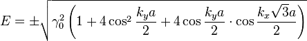
with the nearest-neighbor hopping energy γ0 ≈ 2.8 eV and the lattice constant a ≈ 2.46 Å. The conduction and valence bands, respectively, correspond to the different signs. Two of the six Dirac points are independent, while the rest are equivalent by symmetry. In the vicinity of the K-points the energy depends linearly on the wave vector, similar to a relativistic particle.[65][67] Since an elementary cell of the lattice has a basis of two atoms, the wave function has an effective 2-spinor structure.
As a consequence, at low energies, even neglecting the true spin, the electrons can be described by an equation that is formally equivalent to the massless Dirac equation. Hence, the electrons and holes are called Dirac fermions.[65] This pseudo-relativistic description is restricted to the chiral limit, i.e., to vanishing rest mass M0, which leads to interesting additional features:[65][68]

Here vF ~ 106 m/s (.003 c) is the Fermi velocity in graphene, which replaces the velocity of light in the Dirac theory;  is the vector of the Pauli matrices,
  is the two-component wave function of the electrons, and E is their energy.[63]
The equation describing the electrons' linear dispersion relation is
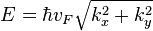 ;
;
where the wavevector k is measured from the Dirac points (the zero of energy is chosen here to coincide with the Dirac points). The equation uses a pseudospin matrix formula that describes two sublattices of the honeycomb lattice.[67]
Single-atom wave propagation
Electron waves in graphene propagate within a single-atom layer, making them sensitive to the proximity of other materials such as high-κ dielectrics, superconductors and ferromagnetics.
Electron transport
Experimental results from transport measurements show that graphene has a remarkable electron mobility at room temperature, with reported values in excess of 15,000 cm2⋅V−1⋅s−1.[35] Additionally, the symmetry of the experimentally measured conductance indicates that hole and electron mobilities should be nearly the same.[64] The mobility is nearly independent of temperature between 10 K and 100 K,[26][69][70] which implies that the dominant scattering mechanism is defect scattering. Scattering by the acoustic phonons of graphene intrinsically limits room temperature mobility to 200,000 cm2⋅V−1⋅s−1 at a carrier density of 1012 cm−2,[70][71] which was later demonstrated and is 10 times greater than copper.[72]
The corresponding resistivity of the graphene sheet would be 10−6 Ω⋅cm. This is less than the resistivity of silver, the lowest known at room temperature.[73] However, for room temperature graphene on SiO
2 substrates, scattering of electrons by optical phonons of the substrate is a larger effect than scattering by graphene’s own phonons. This limits mobility to 40,000 cm2⋅V−1⋅s−1.[70]
Electrical resistance in 40-nanometer-wide nanoribbons of epitaxial graphene changes in discrete steps. The ribbons' conductance exceeds predictions by a factor of 10. The ribbons can act more like optical waveguides or quantum dots, allowing electrons to flow smoothly along the ribbon edges. In copper, resistance increases in proportion to length as electrons encounter impurities.[74][75]
Transport is dominated by two modes. One is ballistic and temperature independent, while the other is thermally activated. Ballistic electrons resemble those in cylindrical carbon nanotubes. At room temperature, resistance increases abruptly at a particular length—the ballistic mode at 16 micrometres and the other at 160 nanometres (1% of the former length).[74]
The ribbons were grown on the edges of three-dimensional structures etched into silicon carbide wafers. When the wafers are heated to approximately 1,000 °C (1,270 K; 1,830 °F), silicon is preferentially driven off along the edges, forming nanoribbons whose structure is determined by the pattern of the three-dimensional surface. The nanoribbons had perfectly smooth edges, annealed by the fabrication process. Electron mobility measurements surpassing one million correspond to a sheet resistance of one ohm per square— two orders of magnitude lower than in two-dimensional graphene.[74]
Graphene electrons can cover micrometer distances without scattering, even at room temperature.[63]
Despite zero carrier density near the Dirac points, graphene exhibits a minimum conductivity on the order of  . The origin of this minimum conductivity is still unclear. However, rippling of the graphene sheet or ionized impurities in the SiO
2 substrate may lead to local puddles of carriers that allow conduction.[64] Several theories suggest that the minimum conductivity should be  ; however, most measurements are of order or greater[35] and depend on impurity concentration.[76]
Near zero carrier density graphene exhibits positive photoconductivity and negative photoconductivity at high carrier density. This is governed by the interplay between photoinduced changes of both the Drude weight and the carrier scattering rate.[77]
Graphene doped with various gaseous species (both acceptors and donors) can be returned to an undoped state by gentle heating in vacuum.[76][78] Even for dopant concentrations in excess of 1012 cm−2 carrier mobility exhibits no observable change.[78] Graphene doped with potassium in ultra-high vacuum at low temperature can reduce mobility 20-fold.[76][79] The mobility reduction is reversible on heating the graphene to remove the potassium.
Due to graphene's two dimensions, charge fractionalization (where the apparent charge of individual pseudoparticles in low-dimensional systems is less than a single quantum[80]) is thought to occur. It may therefore be a suitable material for constructing quantum computers[81] using anyonic circuits.[82]
Anomalous quantum Hall effect
The quantum Hall effect is a quantum mechanical version of the Hall effect, which is the production of transverse (perpendicular to the main current) conductivity in the presence of a magnetic field. The quantization of the Hall effect  at integer multiples (the "Landau level") of the basic quantity
  (where e is the elementary electric charge and h is Planck's constant) It can usually be observed only in very clean silicon or gallium arsenide solids at temperatures around 3 K and very high magnetic fields.
Graphene shows the quantum Hall effect with respect to conductivity quantization: the effect is anomalous in that the sequence of steps is shifted by 1/2 with respect to the standard sequence and with an additional factor of 4. Graphene's Hall conductivity is  , where N is the Landau level and the double valley and double spin degeneracies give the factor of 4.[35] These anomalies are present at room temperature, i.e. at roughly 20 °C (293 K).[26]
This behavior is a direct result of graphene's massless Dirac electrons. In a magnetic field, their spectrum has a Landau level with energy precisely at the Dirac point. This level is a consequence of the Atiyah–Singer index theorem and is half-filled in neutral graphene,[65] leading to the "+1/2" in the Hall conductivity.[27] Bilayer graphene also shows the quantum Hall effect, but with only one of the two anomalies (i.e.  ). In the second anomaly, the first plateau at N=0 is absent, indicating that bilayer graphene stays metallic at the neutrality point.[35]
Unlike normal metals, graphene's longitudinal resistance shows maxima rather than minima for integral values of the Landau filling factor in measurements of the Shubnikov–de Haas oscillations, whereby the term integral quantum Hall effect. These oscillations show a phase shift of π, known as Berry’s phase.[26][64] Berry’s phase arises due to the zero effective carrier mass near the Dirac points.[28] The temperature dependence of the oscillations reveals that the carriers have a non-zero cyclotron mass, despite their zero effective mass.[26]
Graphene samples prepared on nickel films, and on both the silicon face and carbon face of silicon carbide, show the anomalous effect directly in electrical measurements.[83][84][85][86][87][88] Graphitic layers on the carbon face of silicon carbide show a clear Dirac spectrum in angle-resolved photoemission experiments, and the effect is observed in cyclotron resonance and tunneling experiments.[89]
Strong magnetic fields
In magnetic fields above 10 Teslas or so additional plateaus of the Hall conductivity at σxy = νe2/h with ν = 0, ±1, ±4 are observed.[90] A plateau at ν = 3[91] and the fractional quantum Hall effect at ν = 1⁄3 were also reported.[91][92]
These observations with ν = 0, ±1, ±3, ±4 indicate that the four-fold degeneracy (two valley and two spin degrees of freedom) of the Landau energy levels is partially or completely lifted.
Casimir effect
The Casimir effect is an interaction between disjoint neutral bodies provoked by the fluctuations of the electrodynamical vacuum. Mathematically it can be explained by considering the normal modes of electromagnetic fields, which explicitly depend on the boundary (or matching) conditions on the interacting bodies' surfaces. Since graphene/electromagnetic field interaction is strong for a one-atom-thick material, the Casimir effect is of growing interest.[93][94]
van der Waals force
The van der Waals force (or dispersion force) is also unusual, obeying an inverse cubic, asymptotic power law in contrast to the usual inverse quartic.[95]
"Massive" electrons
Graphene's unit cell has two identical carbon atoms and two zero-energy states: one in which the electron resides on atom A, the other in which the electron resides on atom B. Both states exist at exactly zero energy. However, if the two atoms in the unit cell are not identical, the situation changes. Hunt et al. show that placing hBN in contact with graphene can alter the potential felt at atom A versus atom B enough that the electrons develop a mass and accompanying band gap of about 30 meV.[96]
The mass can be positive or negative. An arrangement that slightly raises the energy of an electron on atom A relative to atom B gives it a positive mass, while an arrangement that raises the energy of atom B produces a negative electron mass. The two versions behave alike and are indistinguishable via optical spectroscopy. An electron traveling from a positive-mass region to a negative-mass region must cross an intermediate region where its mass once again becomes zero. This region is gapless and therefore metallic. Metallic modes bounding semiconducting regions of opposite-sign mass is a hallmark of a topological phase and display much the same physics as topological insulators.[96]
If the mass in graphene can be controlled, electrons can be confined to massless regions by surrounding them with massive regions, allowing the patterning of quantum dots, wires, and other mesoscopic structures. It also produces one-dimensional conductors along the boundary. These wires would be protected against backscattering and could carry currents without dissipation.[96]
Optical

Graphene's unique optical properties produce an unexpectedly high opacity for an atomic monolayer in vacuum, absorbing πα ≈ 2.3% of red light, where α is the fine-structure constant.[99] This is a consequence of the "unusual low-energy electronic structure of monolayer graphene that features electron and hole conical bands meeting each other at the Dirac point... [which] is qualitatively different from more common quadratic massive bands."[98] Based on the Slonczewski–Weiss–McClure (SWMcC) band model of graphite, the interatomic distance, hopping value and frequency cancel when optical conductance is calculated using Fresnel equations in the thin-film limit.
Although confirmed experimentally, the measurement is not precise enough to improve on other techniques for determining the fine-structure constant.[100]
Graphene's band gap can be tuned from 0 to 0.25 eV (about 5 micrometre wavelength) by applying voltage to a dual-gate bilayer graphene field-effect transistor (FET) at room temperature.[101] The optical response of graphene nanoribbons is tunable into the terahertz regime by an applied magnetic field.[102] Graphene/graphene oxide systems exhibit electrochromic behavior, allowing tuning of both linear and ultrafast optical properties.[103]
A graphene-based Bragg grating (one-dimensional photonic crystal) has been fabricated and demonstrated its capability for excitation of surface electromagnetic waves in the periodic structure by using 633 nm He–Ne laser as the light source.[104]
Saturable absorption
Such unique absorption could become saturated when the input optical intensity is above a threshold value. This nonlinear optical behavior is termed saturable absorption and the threshold value is called the saturation fluence. Graphene can be saturated readily under strong excitation over the visible to near-infrared region, due to the universal optical absorption and zero band gap. This has relevance for the mode locking of fiber lasers, where fullband mode locking has been achieved by graphene-based saturable absorber. Due to this special property, graphene has wide application in ultrafast photonics. Moreover, the optical response of graphene/graphene oxide layers can be tuned electrically.[103][105] Saturable absorption in graphene could occur at the Microwave and Terahertz band, owing to its wideband optical absorption property. The microwave saturable absorption in graphene demonstrates the possibility of graphene microwave and terahertz photonics devices, such as microwave saturable absorber, modulator, polarizer, microwave signal processing and broad-band wireless access networks.[106]
Nonlinear Kerr effect
Under more intensive laser illumination, graphene could also possess a nonlinear phase shift due to the optical nonlinear Kerr effect. Based on a typical open and close aperture z-scan measurement, graphene possesses a giant non-linear Kerr coefficient of 10−7 cm2⋅W−1, almost nine orders of magnitude larger than that of bulk dielectrics.[107] This suggests that graphene may be a powerful nonlinear Kerr medium, with the possibility of observing a variety of nonlinear effects, the most important of which is the soliton.[108]
Excitonic
First-principle calculations with quasiparticle corrections and many-body effects are performed to study the electronic and optical properties of graphene-based materials. The approach is described as three stages.[109] With GW calculation, the properties of graphene-based materials are accurately investigated, including graphene,[110] graphene nanoribbons,[111] edge and surface functionalized armchair graphene nanoribbons,[112] hydrogen saturated armchair graphene nanoribbons,[113] Josephson effect in graphene SNS junctions with single localized defect[114] and scaling properties in armchair graphene nanoribbons.[115]
Stability
Ab initio calculations show that a graphene sheet is thermodynamically unstable if its size is less than about 20 nm ("graphene is the least stable structure until about 6000 atoms") and becomes the most stable fullerene (as within graphite) only for molecules larger than 24,000 atoms.[116]
Thermal conductivity
Thermal transport in graphene is an active area of research, which has attracted attention because of the potential for thermal management applications. Early measurements of the thermal conductivity of suspended graphene reported an exceptionally large thermal conductivity of approximately 5,300 W⋅m−1⋅K−1,[117] compared with the thermal conductivity of pyrolytic graphite of approximately 2,000 W⋅m−1⋅K−1 at room temperature.[118] However, later studies have questioned whether this ultrahigh value had been overestimated, and have instead measured a wide range of thermal conductivities between 1,500 – 2,500 W⋅m−1⋅K−1 for suspended single layer graphene.[119][120][121][122] The large range in the reported thermal conductivity can be caused by large measurement uncertainties as well as variations in the graphene quality and processing conditions. In addition, it is known that when single-layer graphene is supported on an amorphous material, the thermal conductivity is reduced to about 500 – 600 W⋅m−1⋅K−1 at room temperature as a result of scattering of graphene lattice waves by the substrate,[123][124] and can be even lower for few layer graphene encased in amorphous oxide.[125] Likewise, polymeric residue can contribute to a similar decrease in the thermal conductivity of suspended graphene to approximately 500 – 600 W⋅m−1⋅K−1for bilayer graphene.[126]
It has been suggested that the isotopic composition, the ratio of 12C to 13C, has a significant impact on the thermal conductivity. For example, isotopically pure 12C graphene has higher thermal conductivity than either a 50:50 isotope ratio or the naturally occurring 99:1 ratio.[127] It can be shown by using the Wiedemann–Franz law, that the thermal conduction is phonon-dominated.[117] However, for a gated graphene strip, an applied gate bias causing a Fermi energy shift much larger than kBT can cause the electronic contribution to increase and dominate over the phonon contribution at low temperatures. The ballistic thermal conductance of graphene is isotropic.[128][129]
Potential for this high conductivity can be seen by considering graphite, a 3D version of graphene that has basal plane thermal conductivity of over a 1000 W⋅m−1⋅K−1 (comparable to diamond). In graphite, the c-axis (out of plane) thermal conductivity is over a factor of ~100 smaller due to the weak binding forces between basal planes as well as the larger lattice spacing.[130] In addition, the ballistic thermal conductance of graphene is shown to give the lower limit of the ballistic thermal conductances, per unit circumference, length of carbon nanotubes.[131]
Despite its 2-D nature, graphene has 3 acoustic phonon modes. The two in-plane modes (LA, TA) have a linear dispersion relation, whereas the out of plane mode (ZA) has a quadratic dispersion relation. Due to this, the T2 dependent thermal conductivity contribution of the linear modes is dominated at low temperatures by the T1.5 contribution of the out of plane mode.[131] Some graphene phonon bands display negative Grüneisen parameters.[132] At low temperatures (where most optical modes with positive Grüneisen parameters are still not excited) the contribution from the negative Grüneisen parameters will be dominant and thermal expansion coefficient (which is directly proportional to Grüneisen parameters) negative. The lowest negative Grüneisen parameters correspond to the lowest transverse acoustic ZA modes. Phonon frequencies for such modes increase with the in-plane lattice parameter since atoms in the layer upon stretching will be less free to move in the z direction. This is similar to the behavior of a string, which, when it is stretched, will have vibrations of smaller amplitude and higher frequency. This phenomenon, named "membrane effect," was predicted by Lifshitz in 1952.[133]
Mechanical
The carbon–carbon bond length in graphene is about 0.142 nanometers.[134] Graphene sheets stack to form graphite with an interplanar spacing of 0.335 nm.
Graphene is the strongest material ever tested,[135] with an intrinsic Tensile strength of 130 GPa and a Young's modulus (stiffness) of 1 TPa (150,000,000 psi).[136] The Nobel announcement illustrated this by saying that a 1 square meter graphene hammock would support a 4 kg cat but would weigh only as much as one of the cat's whiskers, at 0.77 mg (about 0.001% of the weight of 1 m2 of paper).[137] I
The spring constant of suspended graphene sheets has been measured using an atomic force microscope (AFM). Graphene sheets were suspended over SiO
2 cavities where an AFM tip was used to apply a stress to the sheet to test its mechanical properties. Its spring constant was in the range 1–5 N/m and the stiffness was 0.5 TPa, which differs from that of bulk graphite. These intrinsic properties could lead to applications such as NEMS as pressure sensors and resonators.[138]
Due to its large surface energy and out of plane ductility, flat graphene sheets are unstable with respect to scrolling, i.e. bending into a cylindrical shape, which is its lower-energy state.[139]
As is true of all materials, regions of graphene are subject to thermal and quantum fluctuations in relative displacement. Although the amplitude of these fluctuations is bounded in 3D structures (even in the limit of infinite size), the Mermin–Wagner theorem shows that the amplitude of long-wavelength fluctuations grows logarithmically with the scale of a 2D structure, and would therefore be unbounded in structures of infinite size. Local deformation and elastic strain are negligibly affected by this long-range divergence in relative displacement. It is believed that a sufficiently large 2D structure, in the absence of applied lateral tension, will bend and crumple to form a fluctuating 3D structure. Researchers have observed ripples in suspended layers of graphene,[30] and it has been proposed that the ripples are caused by thermal fluctuations in the material. As a consequence of these dynamical deformations, it is debatable whether graphene is truly a 2D structure.[35][53][54][140] It has recently been shown that these ripples, if amplified through the introduction of vacancy defects, can impart a negative Poisson's ratio into graphene, resulting in the thinnest auxetic material known so far.[141]
Fracture Toughness
In 2014, researchers from Rice University and the Georgia Institute of Technology have indicated that despite its strength, graphene is also relatively brittle, with a fracture toughness of ~4 MPa√m.[142] This indicates that imperfect graphene is likely to crack in a brittle manner like ceramic materials, as opposed to many metallic materials which tend to have fracture toughnesses in the range of 15–50 MPa√m. Later in 2014, the Rice team announced that graphene showed a greater ability to distribute force from an impact than any known material, 10x that of steel per unit weight.[143] The force was transmitted at 22.2 kilometres per second (13.8 mi/s).[144]
Spin transport
Graphene is claimed to be an ideal material for spintronics due to its small spin-orbit interaction and the near absence of nuclear magnetic moments in carbon (as well as a weak hyperfine interaction). Electrical spin current injection and detection has been demonstrated up to room temperature.[145][146][147] Spin coherence length above 1 micrometre at room temperature was observed,[145] and control of the spin current polarity with an electrical gate was observed at low temperature.[146]
Strong magnetic fields
Graphene's quantum Hall effect in magnetic fields above 10 Teslas or so reveals additional interesting features. Additional plateaus of the Hall conductivity at  with
with  are observed.[90] Also, the observation of a plateau at
  [91] and the fractional quantum Hall effect at
  were reported.[91][92]
These observations with  indicate that the four-fold degeneracy (two valley and two spin degrees of freedom) of the Landau energy levels is partially or completely lifted. One hypothesis is that the magnetic catalysis of symmetry breaking is responsible for lifting the degeneracy.
Spintronic and magnetic properties can present in graphene simultaneously.[148] Low-defect graphene nanomeshes manufactured by using a non-lithographic method exhibit large-amplitude ferromagnetism even at room temperature. Additionally a spin pumping effect is found for fields applied in parallel with the planes of few-layer ferromagnetic nanomeshes, while a magnetoresistance hysteresis loop is observed under perpendicular fields.
Magnetic
In 2014 researchers magnetized graphene by placing it on an atomically smooth layer of magnetic yttrium iron garnet. The graphene's electronic properties were unaffected. Prior approaches involved doping graphene with other substances. The dopant's presence negatively affected its electronic properties.[149]
Biological
In 2015 researchers used graphene to create sensitive bisensors by using epitaxial graphene on silicon carbide. The sensors bind to the 8-hydroxydeoxyguanosine (8-OHdG) and is capable of selective binding with antibodies. The presence of 8-OHdG in blood, urine and saliva is commonly associated with DNA damage. Elevated levels of 8-OHdG have been linked to increased risk of developing several cancers.[150]
Forms
Nanostripes
Graphene nanoribbons ("nanostripes" in the "zig-zag" orientation), at low temperatures, show spin-polarized metallic edge currents, which also suggests applications in the new field of spintronics. (In the "armchair" orientation, the edges behave like semiconductors.[63])
Oxide
Using paper-making techniques on dispersed, oxidized and chemically processed graphite in water, the monolayer flakes form a single sheet and create strong bonds. These sheets, called graphene oxide paper have a measured tensile modulus of 32 GPa.[151] The chemical property of graphite oxide is related to the functional groups attached to graphene sheets. These can change the polymerization pathway and similar chemical processes.[152] Graphene oxide flakes in polymers display enhanced photo-conducting properties.[153] Graphene is normally hydrophobic and impermeable to all gases and liquids (vacuum-tight). However when formed into graphene oxide-based capillary membrane, both liquid water and water vapor flow through as quickly as if the membrane was not present.[154]
Chemical modification

Soluble fragments of graphene can be prepared in the laboratory[155] through chemical modification of graphite. First, microcrystalline graphite is treated with an acidic mixture of sulfuric acid and nitric acid. A series of oxidation and exfoliation steps produce small graphene plates with carboxyl groups at their edges. These are converted to acid chloride groups by treatment with thionyl chloride; next, they are converted to the corresponding graphene amide via treatment with octadecylamine. The resulting material (circular graphene layers of 5.3 angstrom thickness) is soluble in tetrahydrofuran, tetrachloromethane and dichloroethane.
Refluxing single-layer graphene oxide (SLGO) in solvents leads to size reduction and folding of individual sheets as well as loss of carboxylic group functionality, by up to 20%, indicating thermal instabilities of SLGO sheets dependent on their preparation methodology. When using thionyl chloride, acyl chloride groups result, which can then form aliphatic and aromatic amides with a reactivity conversion of around 70–80%.

Hydrazine reflux is commonly used for reducing SLGO to SLG(R), but titrations show that only around 20–30% of the carboxylic groups are lost, leaving a significant number available for chemical attachment. Analysis of SLG(R) generated by this route reveals that the system is unstable and using a room temperature stirring with HCl (< 1.0 M) leads to around 60% loss of COOH functionality. Room temperature treatment of SLGO with carbodiimides leads to the collapse of the individual sheets into star-like clusters that exhibited poor subsequent reactivity with amines (ca. 3–5% conversion of the intermediate to the final amide).[156] It is apparent that conventional chemical treatment of carboxylic groups on SLGO generates morphological changes of individual sheets that leads to a reduction in chemical reactivity, which may potentially limit their use in composite synthesis. Therefore, chemical reactions types have been explored. SLGO has also been grafted with polyallylamine, cross-linked through epoxy groups. When filtered into graphene oxide paper, these composites exhibit increased stiffness and strength relative to unmodified graphene oxide paper.[157]
Full hydrogenation from both sides of graphene sheet results in graphane, but partial hydrogenation leads to hydrogenated graphene.[158] Similarly, both-side fluorination of graphene (or chemical and mechanical exfoliation of graphite fluoride) leads to fluorographene (graphene fluoride),[159] while partial fluorination (generally halogenation) provides fluorinated (halogenated) graphene.
Ligand/ Complex
Graphene can be a huge ligand to coordinate metals and metal ions by introducing functional groups. Structures of graphene ligands are similar to e.g. metal-porphyrin complex, metal-phthalocyanine complex, and metal-phenanthroline complex. Copper and nickel ions has been coordinated with graphene ligands.[160][161]
Bilayer
Bilayer graphene displays the anomalous quantum Hall effect, a tunable band gap[162] and potential for excitonic condensation[163] –making it a promising candidate for optoelectronic and nanoelectronic applications. Bilayer graphene typically can be found either in twisted configurations where the two layers are rotated relative to each other or graphitic Bernal stacked configurations where half the atoms in one layer lie atop half the atoms in the other. Stacking order and orientation govern the optical and electronic properties of bilayer graphene.
One way to synthesize bilayer graphene is via chemical vapor deposition, which can produce large bilayer regions that almost exclusively conform to a Bernal stack geometry.[164]
Fiber
In 2011, Xinming Li and Hongwei Zhu from Tsinghua University reported a novel yet simple approach to fabricate graphene fibers from chemical vapor deposition grown graphene films.[165] The method was scalable and controllable, delivering tunable morphology and pore structure by controlling the evaporation of solvents with suitable surface tension. Flexible all-solid-state supercapacitors based on this graphene fibers were demonstrated in 2013.[166]
3D
In 2013, a three-dimensional honeycomb of hexagonally arranged carbon was termed 3D graphene, although self-supporting 3D graphene has not yet been produced.[167] However 3D chemically modified graphene is a self-supporting material that is characterised as ultralight cellular network ( >1 mg/cm³).[168]
Reinforced
Graphene reinforced with embedded carbon nanotube reinforcing bars (“rebar”) is easier to manipulate, while improving the electrical and mechanical qualities of both materials.[169][170]
Functionalized single- or multiwalled carbon nanotubes are spin-coated on copper foils and then heated and cooled, using the nanotubes themselves as the carbon source. Under heating, the functional carbon groups decompose into graphene, while the nanotubes partially split and form in-plane covalent bonds with the graphene, adding strength. π–π stacking domains add more strength. The nanotubes can overlap, making the material a better conductor than standard CVD-grown graphene. The nanotubes effectively bridge the grain boundaries found in conventional graphene. The technique eliminates the traces of substrate on which later-separated sheets were deposited using epitaxy.[169]
Stacks of a few layers, have been proposed as a cost-effective and physically flexible replacement for indium tin oxide (ITO) used in displays and photovoltaic cells.[169]
Production techniques
Isolated 2D crystals cannot be grown via chemical synthesis beyond small sizes even in principle, because the rapid growth of phonon density with increasing lateral size forces 2D crystallites to bend into the third dimension.[17] However, other routes to 2d materials exist:
Fundamental forces place seemingly insurmountable barriers in the way of creating [2D crystals]... The nascent 2D crystallites try to minimize their surface energy and inevitably morph into one of the rich variety of stable 3D structures that occur in soot.But there is a way around the problem. Interactions with 3D structures stabilize 2D crystals during growth. So one can make 2D crystals sandwiched between or placed on top of the atomic planes of a bulk crystal. In that respect, graphene already exists within graphite... One can then hope to fool Nature and extract single-atom-thick crystallites at a low enough temperature that they remain in the quenched state prescribed by the original higher-temperature 3D growth.[171]
An expanding set of production techniques has supplmented the early approaches of cleaving multi-layer graphite into single layers or to grow it epitaxially by depositing a layer of carbon onto another material. In all cases, the graphite must bond to some substrate to retain its 2d shape.[17]
Exfoliation
As of 2014 exfoliation produced graphene with the lowest number of defects and highest electron mobility.[72]
Adhesive tape
Cleavage is also known as exfoliation. Achieving single layers typically requires multiple exfoliation steps, each producing a slice with fewer layers, until only one remains. Geim and Novoselov used adhesive tape to split their graphene.
After exfoliation the flakes are deposited on a silicon wafer using "dry deposition." Crystallites larger than 1 mm and visible to the naked eye can be obtained with the technique. It is often referred to as a "scotch tape" or "drawing" method. The latter name appeared because the dry deposition resembles drawing with a piece of graphite.[171]
Wedge-based mechanical exfoliation
Another controlled technique to produce few layers of graphene uses a wedge type of tool[172] to address difficulties of the adhesive tape method. In this method, a sharp single-crystal diamond wedge penetrates onto the graphite source to exfoliate layers. This method uses highly ordered pyrolytic graphite (HOPG) as the starting material. The experiments were supported by molecular dynamic simulations.[173]
Reduction of graphite oxide
Graphite oxide reduction was probably the first method of graphene synthesis. P. Boehm reported producing monolayer flakes of reduced graphene oxide in 1962.[174] Geim acknowledged Boehm's contribution.[175] Rapid heating of graphite oxide and exfoliation yields highly dispersed carbon powder with a few percent of graphene flakes. Reduction of graphite oxide monolayer films, e.g. by hydrazine with annealing in argon/hydrogen, was reported to yield graphene films. However, the quality is lower compared to scotch-tape graphene, due to incomplete removal of functional groups. Furthermore, the oxidation protocol introduces permanent defects due to over-oxidation. The oxidation protocol was enhanced to yield graphene oxide with an almost intact carbon framework that allows efficient removal of functional groups. The measured charge carrier mobility exceeded 1,000 centimetres (393.70 in)/Vs.[176] Spectroscopic analysis of reduced graphene oxide has been conducted.[177][178]
Sugar method
Graphene has also been prepared by using a sole sugar(e.g. glucose, fructose, sucrose etc. ), this substrate-free "bottom-up" synthesis method is known as "Tang-Lau method" in which the sole source is sugar, the process is safer, simpler, and more environmentally friendly compared to traditionally “top-down” method. Another important advantage of Tang-Lau method is control of thickness, ranging from monolayer to multilayers by adjusting growth parameters.[179]
Shearing
In 2014 defect-free, unoxidized graphene-containing liquids were made from graphite using mixers that produce local shear rates greater than 10. Commercial graphene products using the output were announced. The method was claimed to be applicable to boron nitride, Molybdenum disulfide and other layered crystals.[180][181]
Sonication
Applying a layer of graphite oxide film to a DVD and burning it in a DVD writer produced a thin graphene film with high electrical conductivity (1738 siemens per meter) and specific surface area (1520 square meters per gram) that was highly resistant and malleable.[182]
Solvent-aided
Dispersing graphite in a proper liquid medium can produce graphene by sonication. Graphene is separated from graphite by centrifugation,[183] producing graphene concentrations initially up to 0.01 mg/ml in N-methylpyrrolidone (NMP) and later to 2.1 mg/ml in NMP,.[184] Using a suitable ionic liquid as the dispersing liquid medium produced concentrations of 5.33 mg/ml.[185] Graphene concentration produced by this method is very low, because nothing prevents the sheets from restacking due to van der Waals forces. The maximum concentrations achieved are the points at which the van der Waals forces overcome the interactive forces between the graphene sheets and the solvent molecules.
Solvent/surfactant-aided
Adding a surfactant to a solvent prior to sonication prevents restacking by adsorbing to the graphene's surface. This produces a higher graphene concentration, but removing the surfactant requires chemical treatments.
Immiscible liquids
Sonicating graphite at the interface of two immiscible liquids, most notably heptane and water, producing macro-scale graphene films. The graphene sheets are adsorbed to the high energy interface between the heptane and the water, where they are kept from restacking. The graphene remains at the interface even when exposed to force in excess of 300,000 g. The solvents may then be evaporated. The sheets are up to ~95% transparent and conductive.[186]
Epitaxy
Epitaxy refers to the deposition of a crystalline overlayer on a crystalline substrate, where there is registry between the two. In some cases epitaxial graphene layers are coupled to surfaces weakly enough (by Van der Waals forces) to retain the two dimensional electronic band structure of isolated graphene.[187][188] An example of weakly coupled epitaxial graphene is the one grown on SiC.[37]
Graphene monolayers grown on silicon carbide and iridium are weakly coupled to these substrates (how weakly remains debated) and the graphene–substrate interaction can be further passivated.[18]
Silicon carbide
Heating silicon carbide (SiC) to high temperatures (>1100 °C) under low pressures (~10−6 torr) reduces it to graphene.[189] This process produces epitaxial graphene with dimensions dependent upon the size of the wafer. The face of the SiC used for graphene formation, silicon- or carbon-terminated, highly influences the thickness, mobility and carrier density of the resulting graphene.
Graphene's electronic band-structure (so-called Dirac cone structure) was first visualized in this material.[190][191][192] Weak anti-localization is observed in this material, but not in exfoliated graphene produced by the drawing method.[193] Large, temperature-independent mobilities approach those in exfoliated graphene placed on silicon oxide, but lower than mobilities in suspended graphene produced by the drawing method. Even without transfer, graphene on SiC exhibits massless Dirac fermions.[83][84][85][86][87][88][194]
The weak van der Waals force that provides the cohesion of multilayer graphene stacks does not always affect the electronic properties of the individual layers. That is, while the electronic properties of certain multilayered epitaxial graphenes are identical to that of a single layer,[195] in other cases the properties are affected,[190][191] as they are in bulk graphite. This effect is well understood theoretically and is related to the symmetry of the interlayer interactions.[195]
Epitaxial graphene on SiC can be patterned using standard microelectronics methods. A band gap can be created and tuned by laser irradiation.[196]
Metal substrates
The atomic structure of a metal substrate can seed the growth of graphene.
Ruthenium
Graphene grown on ruthenium does not typically produce uniform layer thickness. Bonding between the bottom graphene layer and the substrate may affect layer properties.[197]
Iridium
Graphene grown on iridium is very weakly bonded, uniform in thickness and can be highly ordered. As on many other substrates, graphene on iridium is slightly rippled. Due to the long-range order of these ripples, minigaps in the electronic band-structure (Dirac cone) become visible.[198]
Nickel
High-quality sheets of few-layer graphene exceeding 1 cm2 (0.2 sq in) in area have been synthesized via chemical vapor deposition on thin nickel films using multiple techniques.
The growth of graphene on nickel films through chemical vapor deposition occurs in a few steps. First the thin nickel film is exposed to Argon gas at 900–1000 degrees Celsius. Methane is then mixed into the gas, and the carbon from the methane is absorbed into the nickel film. The nickel–carbon solution is then cooled down in argon gas. During the cooling process the carbon diffuses out of the nickel to form graphene films.[83][199][200][201]
Another used temperatures compatible with conventional CMOS processing, using a nickel-based alloy with gold as catalyst.[202] This process dissolves carbon atoms inside a transition metal melt at a certain temperature and then precipitates the dissolved carbon at lower temperatures as single layer graphene (SLG).
The metal is first melted in contact with a carbon source, possibly a graphite crucible inside which the melt is carried out or graphite powder/chunks that are placed in the melt. Keeping the melt in contact with the carbon at a specific temperature dissolves the carbon atoms, saturating the melt based on the metal–carbon binary phase diagram. Lowering the temperature decreases carbon's solubility and the excess carbon precipitates atop the melt. The floating layer can be either skimmed or frozen for later removal. Using different morphology, including thick graphite, few layer graphene (FLG) and SLG were observed on metal substrate. Raman spectroscopy proved that SLG had grown on nickel substrate. The SLG Raman spectrum featured no D and D′ band, indicating its pristine nature. Since nickel is not Raman active, direct Raman spectroscopy of graphene layers on top of the nickel is achievable.[203]
Another approach covered a sheet of silicon dioxide glass (the substrate) on one side with a nickel film. Graphene deposited via chemical vapor deposition formed into layers on both sides of the film, one on the exposed top side, and one on the underside, sandwiched between nickel and glass. Peeling the nickel and the top layer of graphene left intervening layer of graphene behind on the glass. While the top graphene layer could be harvested from the foil as in earlier methods, the bottom layer was already in place on the glass. The quality and purity of the attached layer was not assessed.[204]
Copper
Copper foil, at room temperature and very low pressure and in the presence of small amounts of methane produces high quality graphene. The growth automatically stops after a single layer forms. Arbitrarily large films can be created.[200][205] The single layer growth is also due to the low concentration of carbon in methane. The process is surface-based rather than relying on absorption into the metal and then diffusion of carbon into graphene layers on the surface.[206] The room temperature process eliminates the need for postproduction steps and reduces production from a ten hour/nine to ten step procedure to a single step that takes five minutes. A chemical reaction between the hydrogen plasma formed from the methane and ordinary air molecules in the chamber generates cyano radicals—carbon–nitrogen molecules without electrons. These charged molecules scour the copper of surface imperfections, providing a pristine substrate. The graphene deposits form lines that merge into each other, forming a seamless sheet that contributes to mechanical and electrical integrity.[207]
Larger hydrocarbons such as ethane and propane produce bilayer coatings.[208] Atmospheric pressure CVD growth produces multilayer graphene on copper (similar to nickel).[209]
The material has fewer defects, which in higher temperature processes result from thermal expansion/contraction.[207] Ballistic transport has been observed in the resulting material.[210]
Sodium ethoxide pyrolysis
Gram-quantities of graphene were produced by the reduction of ethanol by sodium metal, followed by pyrolysis of the ethoxide product and washing with water to remove sodium salts.[211]
Silicon/germanium/hydrogen
A normal silicon wafer coated with a layer of germanium (Ge) dipped in dilute hydrofluoric acid strips the naturally forming germanium oxide groups, creating hydrogen-terminated germanium. Chemical vapor deposition deposits a layer of graphene on top. The graphene can be peeled from the wafer using a dry process and is then ready for use. The wafer can be reused. The graphene is wrinkle-free, high quality and low in defects.[212][213]
Roll-to-roll
In 2014 a two-step roll-to-roll manufacturing process was announced that allows scalable graphene production. The first roll-to-roll step produces the graphene via chemical vapor deposition. The second step binds the graphene to a substrate.[214][215]
Nanotube slicing
Graphene can be created by cutting open carbon nanotubes.[216] In one such method multi-walled carbon nanotubes are cut open in solution by action of potassium permanganate and sulfuric acid.[217] In another method graphene nanoribbons were produced by plasma etching of nanotubes partly embedded in a polymer film.[218]
Carbon dioxide reduction
A highly exothermic reaction combusts magnesium in an oxidation–reduction reaction with carbon dioxide, producing a variety of carbon nanoparticles including graphene and fullerenes. The carbon dioxide reactant may be either solid (dry-ice) or gaseous. The products of this reaction are carbon and magnesium oxide. US patent 8377408 was issued for this process.[219]
Spin coating
In 2014, carbon nanotube-reinforced graphene was made via spin coating and annealing functionalized carbon nanotubes. The resulting material was stronger, flexible and more conductive than conventional graphene.[169]
Supersonic spray
Supersonic acceleration of droplets through a Laval nozzle was used to deposit small droplets of reduced graphene-oxide in suspension on a substrate. The droplets disperse evenly, evaporate rapidly and display reduced flake aggregations. In addition, the topological defects (Stone-Wales defect and C
2 vacancies) originally in the flakes disappeared. The result was a higher quality graphene layer. The energy of the impact stretches the graphene and rearranges its carbon atoms into flawless hexagonal graphene with no need for post-treatment.[220][221] The high amount of energy also allows the graphene droplets to heal any defects in the graphene layer that may occur during this process.[222]
Intercalation
Producing graphene via Intercalation splits graphite into single layer graphene by inserting guest molecules/ions between the graphene layers. Graphite was first intercaled in 1841 using a strong oxidizing or reducing agent that damaged the material's desirable properties. Kovtyukhova developed a widely used oxidative intercalation method in 1999. In 2014, she was able to achieve intercalation using non-oxidizing Brønsted acids (phosphoric, sulfuric, dichloroacetic and alkylsulfonic acids), but without oxidizing agents. The new method has yet to achieve output sufficient for commercialization.[223][224]
Laser
In 2014 a laser-based single-step, scalable approach to graphene production was announced. The technique produced and patterned porous three-dimensional graphene film networks from commercial polymer films. The system used a CO2 infrared laser. The sp3-carbon atoms were photothermally converted to sp2-carbon atoms by pulsed laser irradiation. The result exhibits high electrical conductivity. The material can produce interdigitated electrodes for in-plane microsupercapacitors with specific capacitances of >4 mF cm−2 and power densities of ~9 mW cm−2. Laser-induced production appeared to allow roll-to-roll manufacturing processes and provides a route to electronic and energy storage devices.[225]
Microwave Assisted Oxidation
In 2012, a Microwave-assisted, scalable approach was reported to directly synthesize graphene with different size from graphite in one step.[226][227][228] The resulting graphene does not need any post reduction treatment as it contains very low oxygen functionality. This approach avoids use of potassium permanganate in the reaction mixture. It has been also reported that by microwave radiation assistance, graphene oxide with or without holes can be synthesized by controlling microwave time.[229] This method uses a recipe similar to Hummer's method but uses microwave heating instead of traditional heating. Microwave heating can dramatically shorten the reaction time from days to seconds.
Applications
As of 2015, graphene is not used in commercial applications. However, many uses for graphene have been proposed or are under development, in areas including electronics, biological engineering, filtration, lightweight/strong composite materials, photovoltaics and energy storage.[230] Graphene is often produced as a powder and as a dispersion in a polymer matrix. This dispersion is supposedly suitable for advanced composites,[231] paints and coatings, lubricants, oils and functional fluids, capacitors and batteries, thermal management applications, display materials and packaging, inks and 3D-printers’ materials, and barriers and films.[232]
Health risks
Research at Brown university found that 10 µm few-layered graphene flakes are able to pierce cell membranes in solution. They were observed to initially enter via sharp and jagged points, allowing graphene to be internalized in the cell. The physiological effects of this remain uncertain, and this remains a relatively unexplored field.[233][234]
See also
- Bismuthide
- Borophene
- Cadmium arsenide
- Exfoliated graphite nano-platelets
- Germanene
- Graphane
- Graphyne
- Metal-organic framework
- Molybdenum disulfide
- Molybdenum diselenide
- Nanoribbon
- Penta-graphene
- Silicene
- Solid-state engine
- Stanene
- Two-dimensional polymers
References
- ↑ "graphene definition, meaning – what is graphene in the British English Dictionary & Thesaurus – Cambridge Dictionaries Online". cambridge.org.
- ↑ "Definition of graphene noun from the Oxford Advanced Learner's Dictionary".
- ↑ Andronico, Michael (14 April 2014). "5 Ways Graphene Will Change Gadgets Forever". Laptop.
- ↑ "Graphene properties". www.graphene-battery.net. 29 May 2014. Retrieved 29 May 2014.
- ↑ "This Month in Physics History: October 22, 2004: Discovery of Graphene". APS News. Series II 18 (9): 2. 2009.
- ↑ "The Story of Graphene". http://www.graphene.manchester.ac.uk/explore/the-story-of-graphene/''. The University of Manchester. 10 September 2014. Retrieved 9 October 2014.
- ↑ "The Nobel Prize in Physics 2010". The Nobel Foundation. Retrieved 3 December 2013.
- ↑ "Global Demand for Graphene after Commercial Production to be Enormous, says Report". AZONANO.com. 28 February 2014. Retrieved 24 July 2014.
- ↑ Boehm, H. P.; Setton, R.; Stumpp, E. (1994). "Nomenclature and terminology of graphite intercalation compounds" (PDF). Pure and Applied Chemistry 66 (9): 1893–1901. doi:10.1351/pac199466091893.
- ↑ Boehm, H. P.; Clauss, A.; Fischer, G. O.; Hofmann, U. (1962). "Das Adsorptionsverhalten sehr dünner Kohlenstoffolien". Zeitschrift für anorganische und allgemeine Chemie (in German) 316 (3–4): 119–127. doi:10.1002/zaac.19623160303.
- ↑ Mouras, S. et al. (1987). "Synthesis of first stage graphite intercalation compounds with fluorides". Revue de Chimie Minerale 24: 572.
- ↑ Saito, R.; Fujita, Mitsutaka; Dresselhaus, G.; Dresselhaus, M. (1992). "Electronic structure of graphene tubules based on C60". Physical Review B 46 (3): 1804–1811. Bibcode:1992PhRvB..46.1804S. doi:10.1103/PhysRevB.46.1804.
- ↑ Forbeaux, I.; Themlin, J.-M.; Debever, J.-M. (1998). "Heteroepitaxial graphite on 6H-SiC(0001): Interface formation through conduction-band electronic structure". Physical Review B 58 (24): 16396–16406. Bibcode:1998PhRvB..5816396F. doi:10.1103/PhysRevB.58.16396.
- ↑ Wang, S.; Yata, S.; Nagano, J.; Okano, Y.; Kinoshita, H.; Kikuta, H.; Yamabe, T. (2000). "A new carbonaceous material with large capacity and high efficiency for rechargeable Li-ion batteries". Journal of the Electrochemical Society 147 (7): 2498. doi:10.1149/1.1393559.
- ↑ Simpson, C. D.; Brand, J. Diedrich; Berresheim, Alexander J.; Przybilla, Laurence; Räder, Hans Joachim; Müllen, Klaus (2002). "Synthesis of a Giant 222 Carbon Graphite Sheet". Chemistry – A European Journal 6 (6): 1424–1429. doi:10.1002/1521-3765(20020315)8:6<1424::AID-CHEM1424>3.0.CO;2-Z.
- ↑ "graphene layer". IUPAC Gold Book. International Union of Pure and Applied Chemistry. Retrieved 31 March 2012.
- ↑ 17.0 17.1 17.2 Geim, A. (2009). "Graphene: Status and Prospects". Science 324 (5934): 1530–4. arXiv:0906.3799. Bibcode:2009Sci...324.1530G. doi:10.1126/science.1158877. PMID 19541989.
- ↑ 18.0 18.1 Riedl, C.; Coletti, C.; Iwasaki, T.; Zakharov, A.A.; Starke, U. (2009). "Quasi-Free-Standing Epitaxial Graphene on SiC Obtained by Hydrogen Intercalation". Physical Review Letters 103 (24): 246804. arXiv:0911.1953. Bibcode:2009PhRvL.103x6804R. doi:10.1103/PhysRevLett.103.246804. PMID 20366220.
- ↑ Geim, A. K. (2012). "Graphene Prehistory". Physica Scripta T146: 014003. doi:10.1088/0031-8949/2012/T146/014003.
- ↑ Brodie, B. C. (1859). "On the Atomic Weight of Graphite". Philosophical Transactions of the Royal Society of London 149: 249–259. Bibcode:1859RSPT..149..249B. doi:10.1098/rstl.1859.0013. JSTOR 108699.
- ↑ Debije, P; Scherrer, P (1916). "Interferenz an regellos orientierten Teilchen im Röntgenlicht I". Physikalische Zeitschrift (in German) 17: 277.
- ↑ Friedrich, W (1913). "Eine neue Interferenzerscheinung bei Röntgenstrahlen". Physikalische Zeitschrift (in German) 14: 317.
Hull, AW (1917). "A New Method of X-ray Crystal Analysis". Phys. Rev. 10 (6): 661–696. Bibcode:1917PhRv...10..661H. doi:10.1103/PhysRev.10.661. - ↑ Kohlschütter, V.; Haenni, P. (1919). "Zur Kenntnis des Graphitischen Kohlenstoffs und der Graphitsäure". Zeitschrift für anorganische und allgemeine Chemie (in German) 105 (1): 121–144. doi:10.1002/zaac.19191050109.
- ↑ Bernal, JD (1924). "The Structure of Graphite". Proc. R. Soc. Lond. A106 (740): 749–773. JSTOR 94336.
Hassel, O; Mack, H (1924). "Über die Kristallstruktur des Graphits". Zeitschrift für Physik (in German) 25: 317–337. Bibcode:1924ZPhy...25..317H. doi:10.1007/BF01327534. - ↑ DiVincenzo, D. P.; Mele, E. J. (1984). "Self-Consistent Effective Mass Theory for Intralayer Screening in Graphite Intercalation Compounds". Physical Review B 295 (4): 1685–1694. Bibcode:1984PhRvB..29.1685D. doi:10.1103/PhysRevB.29.1685.
- ↑ 26.0 26.1 26.2 26.3 26.4 26.5 Novoselov, K. S.; Geim, A. K.; Morozov, S. V.; Jiang, D.; Katsnelson, M. I.; Grigorieva, I. V.; Dubonos, S. V.; Firsov, A. A. (2005). "Two-dimensional gas of massless Dirac fermions in graphene". Nature 438 (7065): 197–200. arXiv:cond-mat/0509330. Bibcode:2005Natur.438..197N. doi:10.1038/nature04233. PMID 16281030.
- ↑ 27.0 27.1 Gusynin, V. P.; Sharapov, S. G. (2005). "Unconventional Integer Quantum Hall Effect in Graphene". Physical Review Letters 95 (14): 146801. arXiv:cond-mat/0506575. Bibcode:2005PhRvL..95n6801G. doi:10.1103/PhysRevLett.95.146801. PMID 16241680.
- ↑ 28.0 28.1 28.2 Zhang, Y.; Tan, Y. W.; Stormer, H. L.; Kim, P. (2005). "Experimental observation of the quantum Hall effect and Berry's phase in graphene". Nature 438 (7065): 201–204. arXiv:cond-mat/0509355. Bibcode:2005Natur.438..201Z. doi:10.1038/nature04235. PMID 16281031.
- ↑ Ruess, G.; Vogt, F. (1948). "Höchstlamellarer Kohlenstoff aus Graphitoxyhydroxyd". Monatshefte für Chemie (in German) 78 (3–4): 222–242. doi:10.1007/BF01141527.
- ↑ 30.0 30.1 30.2 30.3 Meyer, J.; Geim, A. K.; Katsnelson, M. I.; Novoselov, K. S.; Booth, T. J.; Roth, S. (2007). "The structure of suspended graphene sheets". Nature 446 (7131): 60–63. arXiv:cond-mat/0701379. Bibcode:2007Natur.446...60M. doi:10.1038/nature05545. PMID 17330039.
- ↑ 31.0 31.1 Boehm, H. P.; Clauss, A.; Fischer, G.; Hofmann, U. (1962). "Surface Properties of Extremely Thin Graphite Lamellae". (PDF). Pergamon Press http://graphenetimes.com/wp-content/uploads/1961/09/BoehmProcCarbon1962.pdf. Missing or empty
|title=(help) - ↑ This paper reports graphitic flakes that give an additional contrast equivalent of down to ~0.4 nm or 3 atomic layers of amorphous carbon. This was the best possible resolution for 1960 TEMs. However, neither then nor today it is possible to argue how many layers were in those flakes. Now we know that the TEM contrast of graphene most strongly depends on focusing conditions.[30] For example, it is impossible to distinguish between suspended monolayer and multilayer graphene by their TEM contrasts, and the only known way is to analyse relative intensities of various diffraction spots. The first reliable TEM observations of monolayers are probably given in refs. 24 and 26 of Geim & Novoselov 2007
- ↑ Oshima, C.; Nagashima, A. (1997). "Ultra-thin epitaxial films of graphite and hexagonal boron nitride on solid surfaces". J. Phys.: Condens. Matter 9: 1–20. Bibcode:1997JPCM....9....1O. doi:10.1088/0953-8984/9/1/004.
- ↑ Geim, A. K.; Kim, P. (April 2008). "Carbon Wonderland". Scientific American.
... bits of graphene are undoubtedly present in every pencil mark
- ↑ 35.0 35.1 35.2 35.3 35.4 35.5 35.6 Geim & Novoselov 2007.
- ↑ "United States Patent: 7071258". US Patent Office. Retrieved 12 January 2014.
- ↑ 37.0 37.1 Novoselov, K. S.; Geim, A. K.; Morozov, S. V.; Jiang, D.; Zhang, Y.; Dubonos, S. V.; Grigorieva, I. V.; Firsov, A. A. (2004). "Electric Field Effect in Atomically Thin Carbon Films" (PDF). Science 306 (5696): 666–669. arXiv:cond-mat/0410550. Bibcode:2004Sci...306..666N. doi:10.1126/science.1102896. PMID 15499015.
- ↑ "The Story of Graphene". October 2014.
Following discussions with colleagues, Andre and Kostya adopted a method that researchers in surface science were using –using simple Sellotape to peel away layers of graphite to expose a clean surface for study under the microscope.
- ↑ Kopelevich, Y.; Torres, J.; Da Silva, R.; Mrowka, F.; Kempa, H.; Esquinazi, P. (2003). "Reentrant Metallic Behavior of Graphite in the Quantum Limit". Physical Review Letters 90 (15): 156402. arXiv:cond-mat/0209406. Bibcode:2003PhRvL..90o6402K. doi:10.1103/PhysRevLett.90.156402. PMID 12732058.
- ↑ Luk’yanchuk, Igor A.; Kopelevich, Yakov (2004). "Phase Analysis of Quantum Oscillations in Graphite". Physical Review Letters 93 (16): 166402. arXiv:cond-mat/0402058. Bibcode:2004PhRvL..93p6402L. doi:10.1103/PhysRevLett.93.166402. PMID 15525015.
- ↑ "Graphene pioneers bag Nobel prize". Institute of Physics, UK. 5 October 2010.
- ↑ "New £60m Engineering Innovation Centre to be based in Manchester". http://www.graphene.manchester.ac.uk/latest.php''. The University of Manchester. 10 September 2014. Retrieved 9 October 2014.
- ↑ Burn-Callander, Rebecca (1 July 2014). "Graphene maker aims to build British, billion-pound venture". Daily Telegraph. Retrieved 24 July 2014.
- ↑ Gibson, Robert (10 June 2014). "Consett firm Thomas Swan sees export success with grapheme". The Journal. Retrieved 23 July 2014.
- ↑ "Global breakthrough: Irish scientists discover how to mass produce ‘wonder material’ graphene". The Journal.ie. 20 April 2014. Retrieved 20 December 2014.
- ↑ Bonaccorso, F.; Colombo, L.; Yu, G.; Stoller, M.; Tozzini, V.; Ferrari, A. C.; Ruoff, R. S.; Pellegrini, V. (2015). "Graphene, related two-dimensional crystals, and hybrid systems for energy conversion and storage". Science 347 (6217): 1246501. doi:10.1126/science.1246501.
- ↑ 47.0 47.1 47.2 47.3 47.4 Cooper, Daniel R.; D’Anjou, Benjamin; Ghattamaneni, Nageswara; Harack, Benjamin; Hilke, Michael; Horth, Alexandre; Majlis, Norberto; Massicotte, Mathieu; Vandsburger, Leron; Whiteway, Eric; Yu, Victor (3 November 2011). "Experimental Review of Graphene" (PDF). ISRN Condensed Matter Physics (International Scholarly Research Network) 2012: 1–56. doi:10.5402/2012/501686. Retrieved February 2015.
- ↑ Kasuya, D.; Yudasaka, M.; Takahashi, K.; Kokai, F.; Iijima, S. (2002). "Selective Production of Single-Wall Carbon Nanohorn Aggregates and Their Formation Mechanism". J. Phys. Chem. B 106 (19): 4947–4951. doi:10.1021/jp020387n.
- ↑ Bernatowicz; T. J. et al. (1996). "Constraints on stellar grain formation from presolar graphite in the Murchison meteorite". Astrophysical Journal 472 (2): 760–782. Bibcode:1996ApJ...472..760B. doi:10.1086/178105.
- ↑ Fraundorf, P.; Wackenhut, M. (2002). "The core structure of presolar graphite onions". Astrophysical Journal Letters 578 (2): L153–156. arXiv:astro-ph/0110585. Bibcode:2002ApJ...578L.153F. doi:10.1086/344633.
- ↑ Zan, Recep; Ramasse, Quentin M.; Bangert, Ursel; Novoselov, Konstantin S. (2012). "Graphene re-knits its holes". Mesoscale and Nanoscale Physics 12 (8): 3936–3940. arXiv:1207.1487v1. Bibcode:2012NanoL..12.3936Z. doi:10.1021/nl300985q.
- ↑ Puiu, Tibi (12 July 2012). "Graphene sheets can repair themselves naturally". ZME Science.
- ↑ 53.0 53.1 Carlsson, J. M. (2007). "Graphene: Buckle or break". Nature Materials 6 (11): 801–2. Bibcode:2007NatMa...6..801C. doi:10.1038/nmat2051. PMID 17972931.
- ↑ 54.0 54.1 Fasolino, A.; Los, J. H.; Katsnelson, M. I. (2007). "Intrinsic ripples in graphene". Nature Materials 6 (11): 858–61. arXiv:0704.1793. Bibcode:2007NatMa...6..858F. doi:10.1038/nmat2011. PMID 17891144.
- ↑ 55.0 55.1 Ishigami, Masa et al. (2007). "Atomic Structure of Graphene on SiO2". Nano Lett 7 (6): 1643–1648. Bibcode:2007NanoL...7.1643I. doi:10.1021/nl070613a. PMID 17497819.
- ↑ Stolyarova, Elena et al. (2007). "High-resolution scanning tunneling microscopy imaging of mesoscopic graphene sheets on an insulating surface". Proceedings of the National Academy of Sciences 104 (22): 9209–9212. arXiv:0705.0833. Bibcode:2007PNAS..104.9209S. doi:10.1073/pnas.0703337104. PMC 1874226. PMID 17517635.
- ↑ Denis, P. A.; Iribarne, F. (2013). "Comparative Study of Defect Reactivity in Graphene". Journal of Physical Chemistry C 117 (37): 19048–19055. doi:10.1021/jp4061945.
- ↑ Yamada, Y.; Murota, K; Fujita, R; Kim, J et al. (2014). "Subnanometer vacancy defects introduced on graphene by oxygen gas". Journal of American Chemical Society 136 (6): 2232–2235. doi:10.1021/ja4117268.
- ↑ Eftekhari, A.; Jafarkhani, P. (2013). "Curly Graphene with Specious Interlayers Displaying Superior Capacity for Hydrogen Storage". Journal of Physical Chemistry C 117 (48): 25845–25851. doi:10.1021/jp410044v.
- ↑ Yamada, Y.; Yasuda, H.; Murota, K.; Nakamura, M.; Sodesawa, T.; Sato, S. (2013). "Analysis of heat-treated graphite oxide by X-ray photoelectron spectroscopy". Journal of Material Science 48 (23): 8171–8198. doi:10.1007/s10853-013-7630-0.
- ↑ Yamada, Y.; Kim, J.; Murota, K.; Matsuo, S.; Sato, S. (2014). "Nitrogen-containing graphene analyzed by X-ray photoelectron spectroscopy". Carbon 70: 59–74. doi:10.1016/j.carbon.2013.12.061.
- ↑ "Thinnest graphene sheets react strongly with hydrogen atoms; thicker sheets are relatively unaffected". Phys.org. 1 February 2013.
- ↑ 63.0 63.1 63.2 63.3 Neto, A Castro; Peres, N. M. R.; Novoselov, K. S.; Geim, A. K.; Geim, A. K. (2009). "The electronic properties of graphene" (PDF). Rev Mod Phys 81: 109–162. arXiv:0709.1163. Bibcode:2009RvMP...81..109C. doi:10.1103/RevModPhys.81.109.
- ↑ 64.0 64.1 64.2 64.3 Charlier, J.-C.; Eklund, P.C.; Zhu, J.; Ferrari, A.C. (2008). Jorio, A.; Dresselhaus and, G.; Dresselhaus, M.S., eds. Electron and Phonon Properties of Graphene: Their Relationship with Carbon Nanotubes. Carbon Nanotubes: Advanced Topics in the Synthesis, Structure, Properties and Applications (Berlin/Heidelberg: Springer-Verlag).
- ↑ 65.0 65.1 65.2 65.3 65.4 Semenoff, G. W. (1984). "Condensed-Matter Simulation of a Three-Dimensional Anomaly". Physical Review Letters 53 (26): 2449–2452. Bibcode:1984PhRvL..53.2449S. doi:10.1103/PhysRevLett.53.2449.
- ↑ Wallace, P.R. (1947). "The Band Theory of Graphite". Physical Review 71 (9): 622–634. Bibcode:1947PhRv...71..622W. doi:10.1103/PhysRev.71.622.
- ↑ 67.0 67.1 Avouris, P.; Chen, Z.; Perebeinos, V. (2007). "Carbon-based electronics". Nature Nanotechnology 2 (10): 605–15. Bibcode:2007NatNa...2..605A. doi:10.1038/nnano.2007.300. PMID 18654384.
- ↑ Lamas, C.A.; Cabra, D.C.; Grandi, N. (2009). "Generalized Pomeranchuk instabilities in graphene". Physical Review B 80 (7): 75108. arXiv:0812.4406. Bibcode:2009PhRvB..80g5108L. doi:10.1103/PhysRevB.80.075108.
- ↑ Morozov, S.V.; Novoselov, K.; Katsnelson, M.; Schedin, F.; Elias, D.; Jaszczak, J.; Geim, A. (2008). "Giant Intrinsic Carrier Mobilities in Graphene and Its Bilayer". Physical Review Letters 100 (1): 016602. arXiv:0710.5304. Bibcode:2008PhRvL.100a6602M. doi:10.1103/PhysRevLett.100.016602. PMID 18232798.
- ↑ 70.0 70.1 70.2 Chen, J. H.; Jang, Chaun; Xiao, Shudong; Ishigami, Masa; Fuhrer, Michael S. (2008). "Intrinsic and Extrinsic Performance Limits of Graphene Devices on SiO
2". Nature Nanotechnology 3 (4): 206–9. doi:10.1038/nnano.2008.58. PMID 18654504. - ↑ Akturk, A.; Goldsman, N. (2008). "Electron transport and full-band electron–phonon interactions in graphene". Journal of Applied Physics 103 (5): 053702. Bibcode:2008JAP...103e3702A. doi:10.1063/1.2890147.
- ↑ 72.0 72.1 Kusmartsev, F. V.; Wu, W. M.; Pierpoint, M. P.; Yung, K. C. (2014). "Application of Graphene within Optoelectronic Devices and Transistors". arXiv:1406.0809 [cond-mat.mtrl-sci].
- ↑ Physicists Show Electrons Can Travel More Than 100 Times Faster in Graphene :: University Communications Newsdesk, University of Maryland. Newsdesk.umd.edu (24 March 2008). Retrieved on 2014-01-12.
- ↑ 74.0 74.1 74.2 "New form of graphene allows electrons to behave like photons". kurzweilai.net.
- ↑ Baringhaus, J.; Ruan, M.; Edler, F.; Tejeda, A.; Sicot, M.; Taleb-Ibrahimi, A.; Li, A. P.; Jiang, Z.; Conrad, E. H.; Berger, C.; Tegenkamp, C.; De Heer, W. A. (2014). "Exceptional ballistic transport in epitaxial graphene nanoribbons". Nature 506 (7488): 349. doi:10.1038/nature12952.
- ↑ 76.0 76.1 76.2 Chen, J. H.; Jang, C.; Adam, S.; Fuhrer, M. S.; Williams, E. D.; Ishigami, M. (2008). "Charged Impurity Scattering in Graphene". Nature Physics 4 (5): 377–381. arXiv:0708.2408. Bibcode:2008NatPh...4..377C. doi:10.1038/nphys935.
- ↑ Light pulses control how graphene conducts electricity. kurzweilai.net. 4 August 2014
- ↑ 78.0 78.1 Schedin, F.; Geim, A. K.; Morozov, S. V.; Hill, E. W.; Blake, P.; Katsnelson, M. I.; Novoselov, K. S. (2007). "Detection of individual gas molecules adsorbed on graphene". Nature Materials 6 (9): 652–655. Bibcode:2007NatMa...6..652S. doi:10.1038/nmat1967. PMID 17660825.
- ↑ Adam, S.; Hwang, E. H.; Galitski, V. M.; Das Sarma, S. (2007). "A self-consistent theory for graphene transport". Proc. Nat. Acad. Sci. USA 104 (47): 18392–7. arXiv:0705.1540. Bibcode:2007PNAS..10418392A. doi:10.1073/pnas.0704772104. PMC 2141788. PMID 18003926.
- ↑ Steinberg, Hadar; Barak, Gilad; Yacoby, Amir et al. (2008). "Charge fractionalization in quantum wires (Letter)". Nature Physics 4 (2): 116–119. arXiv:0803.0744. Bibcode:2008NatPh...4..116S. doi:10.1038/nphys810.
- ↑ Trisetyarso, Agung (2012). "Dirac four-potential tunings-based quantum transistor utilizing the Lorentz force". Quantum Information & Computation 12 (11–12): 989. arXiv:1003.4590. Bibcode:2010arXiv1003.4590T.
- ↑ Pachos, Jiannis K. (2009). "Manifestations of topological effects in graphene". Contemporary Physics 50 (2): 375–389. arXiv:0812.1116. Bibcode:2009ConPh..50..375P. doi:10.1080/00107510802650507.
Franz, M. (5 January 2008). "Fractionalization of charge and statistics in graphene and related structures" (PDF). University of British Columbia. - ↑ 83.0 83.1 83.2 Kim, Kuen Soo; Jang, Houk; Lee, Sang Yoon; Kim, Jong Min; Kim, Kwang S.; Ahn, Jong-Hyun; Kim, Philip; Choi, Jae-Young; Hong, Byung Hee et al. (2009). "Large-scale pattern growth of graphene films for stretchable transparent electrodes". Nature 457 (7230): 706–10. Bibcode:2009Natur.457..706K. doi:10.1038/nature07719. PMID 19145232.
- ↑ 84.0 84.1 Jobst, Johannes; Waldmann, Daniel; Speck, Florian; Hirner, Roland; Maude, Duncan K.; Seyller, Thomas; Weber, Heiko B. (2009). "How Graphene-like is Epitaxial Graphene? Quantum Oscillations and Quantum Hall Effect". Physical Review B 81 (19): 195434. arXiv:0908.1900. Bibcode:2010PhRvB..81s5434J. doi:10.1103/PhysRevB.81.195434.
- ↑ 85.0 85.1 Shen, T.; Gu, J.J.; Xu, M; Wu, Y.Q.; Bolen, M.L.; Capano, M.A.; Engel, L.W.; Ye, P.D. (2009). "Observation of quantum-Hall effect in gated epitaxial graphene grown on SiC (0001)". Applied Physics Letters 95 (17): 172105. arXiv:0908.3822. Bibcode:2009ApPhL..95q2105S. doi:10.1063/1.3254329.
- ↑ 86.0 86.1 Wu, Xiaosong; Hu, Yike; Ruan, Ming; Madiomanana, Nerasoa K; Hankinson, John; Sprinkle, Mike; Berger, Claire; de Heer, Walt A. (2009). "Half integer quantum Hall effect in high mobility single layer epitaxial graphene". Applied Physics Letters 95 (22): 223108. arXiv:0909.2903. Bibcode:2009ApPhL..95v3108W. doi:10.1063/1.3266524.
- ↑ 87.0 87.1 Lara-Avila, Samuel; Kalaboukhov, Alexei; Paolillo, Sara; Syväjärvi, Mikael; Yakimova, Rositza; Fal'ko, Vladimir; Tzalenchuk, Alexander; Kubatkin, Sergey (7 July 2009). "SiC Graphene Suitable For Quantum Hall Resistance Metrology". Science Brevia. arXiv:0909.1193. Bibcode:2009arXiv0909.1193L.
- ↑ 88.0 88.1 Alexander-Webber, J.A.; Baker, A.M.R.; Janssen, T.J.B.M.; Tzalenchuk, A.; Lara-Avila, S.; Kubatkin, S.; Yakimova, R.; Piot, B. A.; Maude, D. K.; Nicholas, R.J. (2013). "Phase Space for the Breakdown of the Quantum Hall Effect in Epitaxial Graphene". Physical Review Letters 111 (9): 096601. arXiv:1304.4897. Bibcode:2013PhRvL.111i6601A. doi:10.1103/PhysRevLett.111.096601. PMID 24033057.
- ↑ Fuhrer, Michael S. (2009). "A physicist peels back the layers of excitement about graphene". Nature 459 (7250): 1037. Bibcode:2009Natur.459.1037F. doi:10.1038/4591037e. PMID 19553953.
- ↑ 90.0 90.1 Zhang, Y.; Jiang, Z.; Small, J. P.; Purewal, M. S.; Tan, Y.-W.; Fazlollahi, M.; Chudow, J. D.; Jaszczak, J. A.; Stormer, H. L.; Kim, P. (2006). "Landau-Level Splitting in Graphene in High Magnetic Fields". Physical Review Letters 96 (13): 136806. arXiv:cond-mat/0602649. Bibcode:2006PhRvL..96m6806Z. doi:10.1103/PhysRevLett.96.136806.
- ↑ 91.0 91.1 91.2 91.3 Du, X.; Skachko, Ivan; Duerr, Fabian; Luican, Adina; Andrei, Eva Y. (2009). "Fractional quantum Hall effect and insulating phase of Dirac electrons in graphene". Nature 462 (7270): 192–195. arXiv:0910.2532. Bibcode:2009Natur.462..192D. doi:10.1038/nature08522. PMID 19829294.
- ↑ 92.0 92.1 Bolotin, K.; Ghahari, Fereshte; Shulman, Michael D.; Stormer, Horst L.; Kim, Philip (2009). "Observation of the fractional quantum Hall effect in graphene". Nature 462 (7270): 196–199. arXiv:0910.2763. Bibcode:2009Natur.462..196B. doi:10.1038/nature08582. PMID 19881489.
- ↑ Bordag, M.; Fialkovsky, I. V.; Gitman, D. M.; Vassilevich, D. V. (2009). "Casimir interaction between a perfect conductor and graphene described by the Dirac model". Physical Review B 80 (24): 245406. arXiv:0907.3242. Bibcode:2009PhRvB..80x5406B. doi:10.1103/PhysRevB.80.245406.
- ↑ Fialkovsky, I. V.; Marachevsky, V.N.; Vassilevich, D. V. (2011). "Finite temperature Casimir effect for graphene". Physical Review B 84 (35446): 35446. arXiv:1102.1757. Bibcode:2011PhRvB..84c5446F. doi:10.1103/PhysRevB.84.035446.
- ↑ Dobson, A.; Rubio, A. (2006). "Asymptotics of the dispersion interaction: analytic benchmarks for van der Waals energy functionals". Physical Review Letters 96 (7): 073201. arXiv:cond-mat/0502422. Bibcode:2006PhRvL..96g3201D. doi:10.1103/PhysRevLett.96.073201.
- ↑ 96.0 96.1 96.2 Fuhrer, M. S. (2013). "Critical Mass in Graphene". Science 340 (6139): 1413–1414. doi:10.1126/science.1240317. PMID 23788788.
- ↑ Zhu, Shou-En; Yuan, Shengjun; Janssen, G. C. A. M. (1 October 2014). "Optical transmittance of multilayer graphene". EPL (Europhysics Letters) 108 (1): 17007. doi:10.1209/0295-5075/108/17007.
- ↑ 98.0 98.1 Nair, R. R.; Blake, P.; Grigorenko, A. N.; Novoselov, K. S.; Booth, T. J.; Stauber, T.; Peres, N. M. R.; Geim, A. K. (6 June 2008). "Fine Structure Constant Defines Visual Transparency of Graphene". Science 320 (5881): 1308–1308. doi:10.1126/science.1156965. PMID 18388259.
- ↑ Kuzmenko, A. B.; Van Heumen, E.; Carbone, F.; Van Der Marel, D. (2008). "Universal infrared conductance of graphite". Physical Review Letters 100 (11): 117401. arXiv:0712.0835. Bibcode:2008PhRvL.100k7401K. doi:10.1103/PhysRevLett.100.117401. PMID 18517825.
- ↑ "Graphene Gazing Gives Glimpse Of Foundations Of Universe". ScienceDaily. 4 April 2008.
- ↑ Zhang, Y.; Tang, Tsung-Ta; Girit, Caglar; Hao, Zhao; Martin, Michael C.; Zettl, Alex; Crommie, Michael F.; Shen, Y. Ron; Wang, Feng (11 June 2009). "Direct observation of a widely tunable bandgap in bilayer graphene". Nature 459 (7248): 820–823. Bibcode:2009Natur.459..820Z. doi:10.1038/nature08105. PMID 19516337.
- ↑ Liu, Junfeng; Wright, A. R.; Zhang, Chao; Ma, Zhongshui (29 July 2008). "Strong terahertz conductance of graphene nanoribbons under a magnetic field". Appl Phys Lett 93 (4): 041106–041110. Bibcode:2008ApPhL..93d1106L. doi:10.1063/1.2964093.
- ↑ 103.0 103.1 Kurum, U.; Liu, Bo; Zhang, Kailiang; Liu, Yan; Zhang, Hao (2011). "Electrochemically tunable ultrafast optical response of graphene oxide". Applied Physics Letters 98 (2): 141103. Bibcode:2011ApPhL..98b1103M. doi:10.1063/1.3540647.
- ↑ Sreekanth, K.V.; Zeng, Shuwen; Shang, Jingzhi; Yong, Ken-Tye; Yu, Ting (2012). "Excitation of surface electromagnetic waves in a graphene-based Bragg grating". Scientific Reports 2: 737. Bibcode:2012NatSR...2E.737S. doi:10.1038/srep00737. PMC 3471096. PMID 23071901.
- ↑ Bao, Qiaoliang; Zhang, Han; Wang, Yu; Ni, Zhenhua; Yan, Yongli; Shen, Ze Xiang; Loh, Kian Ping; Tang, Ding Yuan (2009). "Atomic-Layer Graphene as a Saturable Absorber for Ultrafast Pulsed Lasers" (PDF). Advanced Functional Materials 19 (19): 3077–3083. doi:10.1002/adfm.200901007. Archived from the original (PDF) on 17 July 2011.
Zhang, H.; Tang, D. Y.; Zhao, L. M.; Bao, Q. L.; Loh, K. P. (2009). "Large energy mode locking of an erbium-doped fiber laser with atomic layer graphene" (PDF). Optics Express 17 (20): P17630. arXiv:0909.5536. Bibcode:2009OExpr..1717630Z. doi:10.1364/OE.17.017630. Archived from the original (PDF) on 17 July 2011.
Zhang, H.; Bao, Qiaoliang; Tang, Dingyuan; Zhao, Luming; Loh, Kianping (2009). "Large energy soliton erbium-doped fiber laser with a graphene-polymer composite mode locker" (PDF). Applied Physics Letters 95 (14): P141103. arXiv:0909.5540. Bibcode:2009ApPhL..95n1103Z. doi:10.1063/1.3244206. Archived from the original (PDF) on 17 July 2011.
Zhang, H.; Tang, Dingyuan; Knize, R. J.; Zhao, Luming; Bao, Qiaoliang; Loh, Kian Ping (2010). "Graphene mode locked, wavelength-tunable, dissipative soliton fiber laser". Applied Physics Letters 96 (11): 111112. arXiv:1003.0154. Bibcode:2010ApPhL..96k1112Z. doi:10.1063/1.3367743. Archived from the original (PDF) on 21 May 2010., Zhang (2009). "Graphene: Mode-locked lasers". NPG Asia Materials. doi:10.1038/asiamat.2009.52. - ↑ Zheng, Z.; Zhao, Chujun; Lu, Shunbin; Chen, Yu; Li, Ying; Zhang, Han; Wen, Shuangchun (2012). "Microwave and optical saturable absorption in graphene". Optics Express 20 (21): 23201–23214. Bibcode:2012OExpr..2023201Z. doi:10.1364/OE.20.023201. PMID 23188285.
- ↑ Zhang, H.; Virally, Stéphane; Bao, Qiaoliang; Kian Ping, Loh; Massar, Serge; Godbout, Nicolas; Kockaert, Pascal (2012). "Z-scan measurement of the nonlinear refractive index of graphene". Optics Letters 37 (11): 1856–1858. Bibcode:2012OptL...37.1856Z. doi:10.1364/OL.37.001856. PMID 22660052.
- ↑ H Dong, C Conti, A Marini and F Biancalana, "Terahertz relativistic spatial solitons in doped graphene metamaterials," Journal of Physics B: Atomic, Molecular and Optical Physics 46, 15540 (2013).
- ↑ Onida, Giovanni; Rubio, Angel (2002). "Electronic excitations: Density-functional versus many-body Green's-function approaches". Rev. Mod. Phys. 74 (2): 601–659. Bibcode:2002RvMP...74..601O. doi:10.1103/RevModPhys.74.601.
- ↑ Yang, Li; Deslippe, Jack; Park, Cheol-Hwan; Cohen, Marvin; Louie, Steven (2009). "Excitonic Effects on the Optical Response of Graphene and Bilayer Graphene". Physical Review Letters 103 (18): 186802. arXiv:0906.0969. Bibcode:2009PhRvL.103r6802Y. doi:10.1103/PhysRevLett.103.186802. PMID 19905823.
- ↑ Prezzi, Deborah; Varsano, Daniele; Ruini, Alice; Marini, Andrea; Molinari, Elisa (2008). "Optical properties of graphene nanoribbons: The role of many-body effects". Physical Review B 77 (4): 041404. arXiv:0706.0916. Bibcode:2008PhRvB..77d1404P. doi:10.1103/PhysRevB.77.041404.
Yang, Li; Cohen, Marvin L.; Louie, Steven G. (2007). "Excitonic Effects in the Optical Spectra of Graphene Nanoribbons". Nano Lett. 7 (10): 3112–5. arXiv:0707.2983. Bibcode:2007NanoL...7.3112Y. doi:10.1021/nl0716404. PMID 17824720.
Yang, Li; Cohen, Marvin L.; Louie, Steven G. (2008). "Magnetic Edge-State Excitons in Zigzag Graphene Nanoribbons". Physical Review Letters 101 (18): 186401. Bibcode:2008PhRvL.101r6401Y. doi:10.1103/PhysRevLett.101.186401. PMID 18999843. - ↑ Zhu, Xi; Su, Haibin (2010). "Excitons of Edge and Surface Functionalized Graphene Nanoribbons". J. Phys. Chem. C 114 (41): 17257–17262. doi:10.1021/jp102341b.
- ↑ Wang, Min; Li, Chang Ming (2011). "Excitonic properties of hydrogen saturation-edged armchair graphene nanoribbons". Nanoscale 3 (5): 2324–8. Bibcode:2011Nanos...3.2324W. doi:10.1039/c1nr10095e. PMID 21503364.
- ↑ Bolmatov, Dima; Mou, Chung-Yu (2010). "Josephson effect in graphene SNS junction with a single localized defect". Physica B 405 (13): 2896–2899. arXiv:1006.1391. Bibcode:2010PhyB..405.2896B. doi:10.1016/j.physb.2010.04.015.
Bolmatov, Dima; Mou, Chung-Yu (2010). "Tunneling conductance of the graphene SNS junction with a single localized defect". Journal of Experimental and Theoretical Physics (JETP) 110 (4): 613–617. arXiv:1006.1386. Bibcode:2010JETP..110..613B. doi:10.1134/S1063776110040084. - ↑ Zhu, Xi; Su, Haibin (2011). "Scaling of Excitons in Graphene Nanoribbons with Armchair Shaped Edges". Journal of Physical Chemistry A 115 (43): 11998–12003. doi:10.1021/jp202787h.
- ↑ Shenderova, O. B.; Zhirnov, V. V.; Brenner, D. W. (2002). "Carbon Nanostructures". Critical Reviews in Solid State and Materials Sciences 27 (3–4): 227–356. Bibcode:2002CRSSM..27..227S. doi:10.1080/10408430208500497.
- ↑ 117.0 117.1 Balandin, A. A.; Ghosh, Suchismita; Bao, Wenzhong; Calizo, Irene; Teweldebrhan, Desalegne; Miao, Feng; Lau, Chun Ning (20 February 2008). "Superior Thermal Conductivity of Single-Layer Graphene". Nano Letters ASAP 8 (3): 902–907. Bibcode:2008NanoL...8..902B. doi:10.1021/nl0731872. PMID 18284217.
- ↑ Y S. Touloukian (1970). Thermophysical Properties of Matter: Thermal conductivity : nonmetallic solids. IFI/Plenum. ISBN 978-0-306-67020-6.
- ↑ Cai, Weiwei; Moore, Arden L.; Zhu, Yanwu; Li, Xuesong; Chen, Shanshan; Shi, Li; Ruoff, Rodney S. (2010). "Thermal Transport in Suspended and Supported Monolayer Graphene Grown by Chemical Vapor Deposition". Nano Letters 10 (5): 1645–1651. doi:10.1021/nl9041966. ISSN 1530-6984.
- ↑ Faugeras, Clement; Faugeras, Blaise; Orlita, Milan; Potemski, M.; Nair, Rahul R.; Geim, A. K. (2010). "Thermal Conductivity of Graphene in Corbino Membrane Geometry". ACS Nano 4 (4): 1889–1892. doi:10.1021/nn9016229. ISSN 1936-0851.
- ↑ Xu, Xiangfan; Pereira, Luiz F. C.; Wang, Yu; Wu, Jing; Zhang, Kaiwen; Zhao, Xiangming; Bae, Sukang; Tinh Bui, Cong; Xie, Rongguo; Thong, John T. L.; Hong, Byung Hee; Loh, Kian Ping; Donadio, Davide; Li, Baowen; Özyilmaz, Barbaros (2014). "Length-dependent thermal conductivity in suspended single-layer graphene". Nature Communications 5. doi:10.1038/ncomms4689. ISSN 2041-1723.
- ↑ Lee, Jae-Ung; Yoon, Duhee; Kim, Hakseong; Lee, Sang Wook; Cheong, Hyeonsik (2011). "Thermal conductivity of suspended pristine graphene measured by Raman spectroscopy". Physical Review B 83 (8). doi:10.1103/PhysRevB.83.081419. ISSN 1098-0121.
- ↑ Seol, J. H.; Jo, I.; Moore, A. L.; Lindsay, L.; Aitken, Z. H.; Pettes, M. T.; Li, X.; Yao, Z.; Huang, R.; Broido, D.; Mingo, N.; Ruoff, R. S.; Shi, L. (2010). "Two-Dimensional Phonon Transport in Supported Graphene". Science 328 (5975): 213–216. doi:10.1126/science.1184014. ISSN 0036-8075.
- ↑ Klemens, P. G. (2001). "Theory of Thermal Conduction in Thin Ceramic Films". International Journal of Thermophysics 22 (1): 265–275. doi:10.1023/A:1006776107140. ISSN 0195-928X.
- ↑ Jang, Wanyoung; Chen, Zhen; Bao, Wenzhong; Lau, Chun Ning; Dames, Chris (2010). "Thickness-Dependent Thermal Conductivity of Encased Graphene and Ultrathin Graphite". Nano Letters 10 (10): 3909–3913. doi:10.1021/nl101613u. ISSN 1530-6984.
- ↑ Pettes, Michael Thompson; Jo, Insun; Yao, Zhen; Shi, Li (2011). "Influence of Polymeric Residue on the Thermal Conductivity of Suspended Bilayer Graphene". Nano Letters 11 (3): 1195–1200. doi:10.1021/nl104156y. ISSN 1530-6984.
- ↑ Chen, Shanshan; Wu, Qingzhi; Mishra, Columbia; Kang, Junyong; Zhang, Hengji; Cho, Kyeongjae; Cai, Weiwei; Balandin, Alexander A.; Ruoff, Rodney S. (2012). "Thermal conductivity of isotopically modified graphene". Nature Materials (10 January 2012) 11 (3): 203–207. arXiv:1112.5752. Bibcode:2012NatMa..11..203C. doi:10.1038/nmat3207.
Lay summary: Tracy, Suzanne (12 January 2012). "Keeping Electronics Cool". Scientific Computing (Advantage Business Media). scientificcomputing.com. - ↑ Saito, K.; Nakamura, J.; Natori, A. (2007). "Ballistic thermal conductance of a graphene sheet". Physical Review B 76 (11): 115409. Bibcode:2007PhRvB..76k5409S. doi:10.1103/PhysRevB.76.115409.
- ↑ Liang, Qizhen; Yao, Xuxia; Wang, Wei; Liu, Yan; Wong, Ching Ping (2011). "A Three-Dimensional Vertically Aligned Functionalized Multilayer Graphene Architecture: An Approach for Graphene-Based Thermal Interfacial Materials". ACS Nano 5 (3): 2392–2401. doi:10.1021/nn200181e. PMID 21384860.
- ↑ Delhaes, P. (2001). Graphite and Precursors. CRC Press. ISBN 90-5699-228-7.
- ↑ 131.0 131.1 Mingo, N.; Broido, D.A. (2005). "Carbon Nanotube Ballistic Thermal Conductance and Its Limits". Physical Review Letters 95 (9): 096105. Bibcode:2005PhRvL..95i6105M. doi:10.1103/PhysRevLett.95.096105.
- ↑ Mounet, N.; Marzari, N. (2005). "First-principles determination of the structural, vibrational and thermodynamic properties of diamond, graphite, and derivatives". Physical Review B 71 (20): 205214. arXiv:cond-mat/0412643. Bibcode:2005PhRvB..71t5214M. doi:10.1103/PhysRevB.71.205214.
- ↑ Lifshitz, I.M. (1952). Journal of Experimental and Theoretical Physics (in Russian) 22: 475. Missing or empty
|title=(help) - ↑ Heyrovska, Raji (2008). "Atomic Structures of Graphene, Benzene and Methane with Bond Lengths as Sums of the Single, Double and Resonance Bond Radii of Carbon". arXiv:0804.4086 [physics.gen-ph].
- ↑ Lee, Changgu (2008). "Measurement of the Elastic Properties and Intrinsic Strength of Monolayer Graphene". Science 321 (385): 385–388. doi:10.1126/science.1157996. PMID 18635798.
- ↑ Lee, C.; Wei, X.; Kysar, J. W.; Hone, J. (2008). "Measurement of the Elastic Properties and Intrinsic Strength of Monolayer Graphene". Science 321 (5887): 385–8. Bibcode:2008Sci...321..385L. doi:10.1126/science.1157996. PMID 18635798. Lay summary.
- ↑ "2010 Nobel Physics Laureates" (PDF). nobelprize.org.
- ↑ Frank, I. W.; Tanenbaum, D. M.; Van Der Zande, A.M.; McEuen, P. L. (2007). "Mechanical properties of suspended graphene sheets" (PDF). J. Vac. Sci. Technol. B 25 (6): 2558–2561. Bibcode:2007JVSTB..25.2558F. doi:10.1116/1.2789446.
- ↑ Braga, S.; Coluci, V. R.; Legoas, S. B.; Giro, R.; Galvão, D. S.; Baughman, R. H. (2004). "Structure and Dynamics of Carbon Nanoscrolls". Nano Letters 4 (5): 881–884. Bibcode:2004NanoL...4..881B. doi:10.1021/nl0497272.
- ↑ Bolmatov, Dima; Mou, Chung-Yu (2011). "Graphene-based modulation-doped superlattice structures". Journal of Experimental and Theoretical Physics (JETP) 112: 102–107. arXiv:1011.2850. Bibcode:2011JETP..112..102B. doi:10.1134/S1063776111010043.
Bolmatov, Dima (2011). "Thermodynamic properties of tunneling quasiparticles in graphene-based structures". Physica C 471 (23–24): 1651–1654. arXiv:1106.6331. Bibcode:2011PhyC..471.1651B. doi:10.1016/j.physc.2011.07.008. - ↑ Grima, J. N.; Winczewski, S.; Mizzi, L.; Grech, M. C.; Cauchi, R.; Gatt, R.; Attard, D.; Wojciechowski, K.W.; Rybicki, J. (2014). "Tailoring Graphene to Achieve Negative Poisson's Ratio Properties". Advanced Materials 27: 1455–1459. doi:10.1002/adma.201404106.
- ↑ Zhang, Peng; Ma, Lulu; Fan, Feifei; Zeng, Zhi; Peng, Cheng; Loya, Phillip E.; Liu, Zheng; Gong, Yongji; Zhang, Jiangnan; Zhang, Xingxiang; Ajayan, Pulickel M.; Zhu, Ting; Lou, Jun (2014). "Fracture toughness of graphene". Nature Communications 5. doi:10.1038/ncomms4782. ISSN 2041-1723.
- ↑ Dorrieron, Jason (4 December 2014). "Graphene Armor Would Be Light, Flexible and Far Stronger Than Steel". Singularity Hub. Retrieved December 2014.
- ↑ Coxworth, Ben (1 December 2014). "Graphene could find use in lightweight ballistic body armor". Gizmag. Retrieved December 2014.
- ↑ 145.0 145.1 Tombros, Nikolaos et al. (2007). "Electronic spin transport and spin precession in single graphene layers at room temperature". Nature (PDF) 448 (7153): 571–575. arXiv:0706.1948. Bibcode:2007Natur.448..571T. doi:10.1038/nature06037. PMID 17632544.
- ↑ 146.0 146.1 Cho, Sungjae; Chen, Yung-Fu; Fuhrer, Michael S. (2007). "Gate-tunable Graphene Spin Valve". Applied Physics Letters 91 (12): 123105. arXiv:0706.1597. Bibcode:2007ApPhL..91l3105C. doi:10.1063/1.2784934.
- ↑ Ohishi, Megumi et al. (2007). "Spin Injection into a Graphene Thin Film at Room Temperature". Jpn J Appl Phys 46: L605–L607. arXiv:0706.1451. Bibcode:2007JaJAP..46L.605O. doi:10.1143/JJAP.46.L605.
- ↑ Hashimoto, T.; Kamikawa, S.; Yagi, Y.; Haruyama, J.; Yang, H.; Chshiev, M. (2014). "Graphene edge spins: spintronics and magnetism in graphene nanomeshes" (PDF). Nanosystems: physics, chemistry, mathematics. 5 (1): 25–38.
- ↑ Coxworth, Ben (January 27, 2015). "Scientists give graphene one more quality – magnetism". Gizmag. Retrieved February 2015.
- ↑ Tehrani, Z. (2014-09-01). "Generic epitaxial graphene biosensors for ultrasensitive detection of cancer risk biomarker". doi:10.1088/2053-1583/1/2/025004.
- ↑ "Graphene Oxide Paper". Northwestern University. Archived from the original on 20 July 2011. Retrieved 28 February 2011.
- ↑ Eftekhari, Ali; Yazdani, Bahareh (2010). "Initiating electropolymerization on graphene sheets in graphite oxide structure". Journal of Polymer Science Part A: Polymer Chemistry 48 (10): 2204–2213. Bibcode:2010JPoSA..48.2204E. doi:10.1002/pola.23990.
- ↑ Nalla, Venkatram; Polavarapu, L; Manga, KK; Goh, BM; Loh, KP; Xu, QH; Ji, W (2010). "Transient photoconductivity and femtosecond nonlinear optical properties of a conjugated polymer–graphene oxide composite". Nanotechnology 21 (41): 415203. Bibcode:2010Nanot..21O5203N. doi:10.1088/0957-4484/21/41/415203. PMID 20852355.
- ↑ Nair, R. R.; Wu, H. A.; Jayaram, P. N.; Grigorieva, I. V.; Geim, A. K. (2012). "Unimpeded permeation of water through helium-leak-tight graphene-based membranes". Science 335 (6067): 442–4. arXiv:1112.3488. Bibcode:2012Sci...335..442N. doi:10.1126/science.1211694. PMID 22282806.
- ↑ Niyogi, Sandip; Bekyarova, Elena; Itkis, Mikhail E.; McWilliams, Jared L.; Hamon, Mark A.; Haddon, Robert C. (2006). "Solution Properties of Graphite and Graphene". J. Am. Chem. Soc. 128 (24): 7720–7721. doi:10.1021/ja060680r. PMID 16771469.
- ↑ Whitby, Raymond L.D.; Korobeinyk, Alina; Glevatska, Katya V. (2011). "Morphological changes and covalent reactivity assessment of single-layer graphene oxides under carboxylic group-targeted chemistry". Carbon 49 (2): 722–725. doi:10.1016/j.carbon.2010.09.049.
- ↑ Park, Sungjin; Dikin, Dmitriy A.; Nguyen, SonBinh T.; Ruoff, Rodney S. (2009). "Graphene Oxide Sheets Chemically Cross-Linked by Polyallylamine". J. Phys. Chem. C 113 (36): 15801–15804. doi:10.1021/jp907613s.
- ↑ Elias, D. C.; Nair, R. R.; Mohiuddin, T. M. G.; Morozov, S. V.; Blake, P.; Halsall, M. P.; Ferrari, A. C.; Boukhvalov, D. W.; Katsnelson, M. I.; Geim, A. K.; Novoselov, K. S. (2009). "Control of Graphene's Properties by Reversible Hydrogenation: Evidence for Graphane". Science 323 (5914): 610–3. arXiv:0810.4706. Bibcode:2009Sci...323..610E. doi:10.1126/science.1167130. PMID 19179524.
- ↑ Garcia, J. C.; de Lima, D. B.; Assali, L. V. C.; Justo, J. F. (2011). "Group IV graphene- and graphane-like nanosheets". J. Phys. Chem. C 115: 13242–13246. doi:10.1021/jp203657w.
- ↑ Yamada, Y.; Miyauchi, M.; Kim, J.; Hirose-Takai, K.; Sato, Y.; Suenaga, K.; Ohba, T.; Sodesawa, T.; Sato, S. (2011). "Exfoliated graphene ligands stabilizing copper cations". Carbon 49 (10): 3375. doi:10.1016/j.carbon.2011.03.056.
Yamada, Y.; Miyauchi, M.; Jungpil, K. et al. "Exfoliated graphene ligands stabilizing copper cations". Carbon 49: 3375–3378. doi:10.1016/j.carbon.2011.03.056. - ↑ Yamada, Y.; Suzuki, Y.; Yasuda, H.; Uchizawa, S.; Hirose-Takai, K.; Sato, Y.; Suenaga, K.; Sato, S. (2014). "Functionalized graphene sheets coordinating metal cations". Carbon 75: 81. doi:10.1016/j.carbon.2014.03.036.
Yamada, Y.; Suzuki, Y.; Yasuda, H. et al. "Functionalized graphene sheets coordinating metal cations". Carbon 75: 81–94. doi:10.1016/j.carbon.2014.03.036. - ↑ Min, Hongki; Sahu, Bhagawan; Banerjee, Sanjay; MacDonald, A. (2007). "Ab initio theory of gate induced gaps in graphene bilayers". Physical Review B 75 (15): 155115. arXiv:cond-mat/0612236. Bibcode:2007PhRvB..75o5115M. doi:10.1103/PhysRevB.75.155115.
- ↑ Barlas, Yafis; Côté, R.; Lambert, J.; MacDonald, A. H. (2010). "Anomalous Exciton Condensation in Graphene Bilayers". Physical Review Letters 104 (9): 96802. arXiv:0909.1502. Bibcode:2010PhRvL.104i6802B. doi:10.1103/PhysRevLett.104.096802.
- ↑ Min, Lola; Hovden, Robert; Huang, Pinshane; Wojcik, Michal; Muller, David A.; Park, Jiwoong (2012). "Twinning and Twisting of Tri- and Bilayer Graphene". NanoLetters 12 (3): 1609–1615. Bibcode:2012NanoL..12.1609B. doi:10.1021/nl204547v.
- ↑ Li, Xinming; Zhao, Tianshuo; Wang, Kunlin; Yang, Ying; Wei, Jinquan; Kang, Feiyu; Wu, Dehai; Zhu, Hongwei (29 August 2011). "Directly Drawing Self-Assembled, Porous, and Monolithic Graphene Fiber from Chemical Vapor Deposition Grown Graphene Film and Its Electrochemical Properties". Langmuir 27 (19): 12164–71. doi:10.1021/la202380g. PMID 21875131.
- ↑ "Flexible all solid-state supercapacitors based on chemical vapor deposition derived graphene fibers". 3 September 2013.
- ↑ Wang, H.; Sun, K.; Tao, F.; Stacchiola, D. J.; Hu, Y. H. (2013). "3D Honeycomb-Like Structured Graphene and Its High Efficiency as a Counter-Electrode Catalyst for Dye-Sensitized Solar Cells". Angewandte Chemie 125 (35): 9380. doi:10.1002/ange.201303497.
Wang, Hui; Sun, Kai; Tao, Franklin; Stacchiola, Dario J.; Hu, Yun Hang. "3D graphene could replace expensive platinum in solar cells". Angewandte Chemie (KurzweilAI) 125 (35): 9380–9384. doi:10.1002/ange.201303497. Retrieved 24 August 2013. - ↑ Barg, S.; Perez, F. M.; Ni, N.; Do Vale Pereira, P.; Maher, R. C.; Garcia-Tuñon, E.; Eslava, S.; Agnoli, S.; Mattevi, C.; Saiz, E. (2014). "Mesoscale assembly of chemically modified graphene into complex cellular networks". Nature Communications 5. doi:10.1038/ncomms5328.
- ↑ 169.0 169.1 169.2 169.3 "Carbon nanotubes as reinforcing bars to strengthen graphene and increase conductivity". KurzweilAI. 9 April 2014. Retrieved 23 April 2014.
- ↑ Yan, Z.; Peng, Z.; Casillas, G.; Lin, J.; Xiang, C.; Zhou, H.; Yang, Y.; Ruan, G.; Raji, A. R. O.; Samuel, E. L. G.; Hauge, R. H.; Yacaman, M. J.; Tour, J. M. (2014). "Rebar Graphene". ACS Nano: 140407122527007. doi:10.1021/nn501132n.
- ↑ 171.0 171.1 Geim, A. K.; MacDonald, A. H. (2007). "Graphene: Exploring carbon flatland". Physics Today 60 (8): 35–41. Bibcode:2007PhT....60h..35G. doi:10.1063/1.2774096.
- ↑ Jayasena, Buddhika; Subbiah Sathyan (2011). "A novel mechanical cleavage method for synthesizing few-layer graphenes". Nanoscale Research Letters 6 (95). Bibcode:2011NRL.....6...95J. doi:10.1186/1556-276X-6-95. PMC 3212245. PMID 21711598.
- ↑ Jayasena, B.; Reddy C.D; Subbiah. S (2013). "Separation, folding and shearing of graphene layers during wedge-based mechanical exfoliation". Nanotechnology 24 (20): 205301. Bibcode:2013Nanot..24t5301J. doi:10.1088/0957-4484/24/20/205301.
- ↑ "Boehm’s 1961 isolation of graphene". Graphene Times. 7 December 2009.
- ↑ "Many Pioneers in Graphene Discovery". Letters to the Editor. Aps.org. January 2010.
- ↑ Eigler, S.; Enzelberger-Heim, M.; Grimm, S.; Hofmann, P.; Kroener, W.; Geworski, A.; Dotzer, C.; Röckert, M.; Xiao, J.; Papp, C.; Lytken, O.; Steinrück, H.-P.; Müller, P.; Hirsch, A. (2013). "Wet Chemical Synthesis of Graphene". Advanced Materials 25 (26): 3583–3587. doi:10.1002/adma.201300155. PMID 23703794.
- ↑ Yamada, Y.; Yasuda, H.; Murota, K.; Nakamura, M.; Sodesawa, T.; Sato, S. (2013). "Analysis of heat-treated graphite oxide by X-ray photoelectron spectroscopy". Journal of Materials Science 48 (23): 8171. doi:10.1007/s10853-013-7630-0.
- ↑ Ji, L.; Xin, H. L.; Kuykendall, T. R.; Wu, S. L.; Zheng, H.; Rao, M.; Cairns, E. J.; Battaglia, V.; Zhang, Y. (2012). "SnS2 nanoparticle loaded graphene nanocomposites for superior energy storage". Physical Chemistry Chemical Physics 14 (19): 6981. doi:10.1039/C2CP40790F.
- ↑ Tang, L.; Li, X.; Ji, R.; Teng, K. S.; Tai, G.; Ye, J.; Wei, C.; Lau, S. P. (2012). "Bottom-up synthesis of large-scale graphene oxide nanosheets". Journal of Materials Chemistry 22 (12): 5676. doi:10.1039/C2JM15944A.
- ↑ "A new method of producing large volumes of high-quality graphene". KurzweilAI. 2 May 2014. Retrieved 3 August 2014.
- ↑ Paton, Keith R. (2014). "Scalable production of large quantities of defect-free few-layer graphene by shear exfoliation in liquids". Nature Materials 13 (6): 624–630. doi:10.1038/nmat3944.
- ↑ "Laser Scribing of High-Performance and Flexible Graphene-Based Electrochemical Capacitors". Sciencemag.org. 16 March 2012.
Marcus, Jennifer (15 March 2012). "Researchers develop graphene supercapacitor holding promise for portable electronics / UCLA Newsroom". Newsroom.ucla.edu. - ↑ Hernandez, Y.; Nicolosi, V.; Lotya, M.; Blighe, F. M.; Sun, Z.; De, S.; McGovern, I. T.; Holland, B.; Byrne, M.; Gun'Ko, Y. K.; Boland, J. J.; Niraj, P.; Duesberg, G.; Krishnamurthy, S.; Goodhue, R.; Hutchison, J.; Scardaci, V.; Ferrari, A. C.; Coleman, J. N. (2008). "High-yield production of graphene by liquid-phase exfoliation of graphite". Nature Nanotechnology 3 (9): 563–568. doi:10.1038/nnano.2008.215. PMID 18772919.
- ↑ Alzari, V.; Nuvoli, D.; Scognamillo, S.; Piccinini, M.; Gioffredi, E.; Malucelli, G.; Marceddu, S.; Sechi, M.; Sanna, V.; Mariani, A. (2011). "Graphene-containing thermoresponsive nanocomposite hydrogels of poly(N-isopropylacrylamide) prepared by frontal polymerization". Journal of Materials Chemistry 21 (24): 8727. doi:10.1039/C1JM11076D.
- ↑ Nuvoli, D.; Valentini, L.; Alzari, V.; Scognamillo, S.; Bon, S. B.; Piccinini, M.; Illescas, J.; Mariani, A. (2011). "High concentration few-layer graphene sheets obtained by liquid phase exfoliation of graphite in ionic liquid". Journal of Materials Chemistry 21 (10): 3428. doi:10.1039/C0JM02461A.
- ↑ Woltornist, S. J., Oyer, A. J., Carrillo, J.-M. Y., Dobrynin, A. V, & Adamson, D. H. (2013). Conductive thin films of pristine graphene by solvent interface trapping. ACS nano, 7(8), 7062–6. doi:10.1021/nn402371c
- ↑ Gall, N. R.; Rut'Kov, E. V.; Tontegode, A. Ya. (1997). "Two Dimensional Graphite Films on Metals and Their Intercalation". International Journal of Modern Physics B 11 (16): 1865–1911. Bibcode:1997IJMPB..11.1865G. doi:10.1142/S0217979297000976.
- ↑ Gall, N. R.; Rut'Kov, E. V.; Tontegode, A. Ya. (1995). "Influence of surface carbon on the formation of silicon-refractory metal interfaces". Thin Solid Films 266 (2): 229–233. Bibcode:1995TSF...266..229G. doi:10.1016/0040-6090(95)06572-5.
- ↑ Sutter, P. (2009). "Epitaxial graphene: How silicon leaves the scene". Nature Materials 8 (3): 171–2. Bibcode:2009NatMa...8..171S. doi:10.1038/nmat2392. PMID 19229263.
- ↑ 190.0 190.1 Ohta, T.; Bostwick, Aaron; McChesney, J.; Seyller, Thomas; Horn, Karsten; Rotenberg, Eli (2007). "Interlayer Interaction and Electronic Screening in Multilayer Graphene Investigated with Angle-Resolved Photoemission Spectroscopy". Physical Review Letters 98 (20): 206802. Bibcode:2007PhRvL..98t6802O. doi:10.1103/PhysRevLett.98.206802. PMID 17677726.
- ↑ 191.0 191.1 Bostwick, A.; Ohta, Taisuke; McChesney, Jessica L; Emtsev, Konstantin V; Seyller, Thomas; Horn, Karsten; Rotenberg, Eli (2007). "Symmetry breaking in few layer graphene films". New Journal of Physics 9 (10): 385. arXiv:0705.3705. Bibcode:2007NJPh....9..385B. doi:10.1088/1367-2630/9/10/385.
- ↑ Zhou, S.Y.; Gweon, G.-H.; Graf, J.; Fedorov, A. V.; Spataru, C. D.; Diehl, R. D.; Kopelevich, Y.; Lee, D.-H.; Louie, Steven G.; Lanzara, A. (2006). "First direct observation of Dirac fermions in graphite". Nature Physics 2 (9): 595–599. arXiv:cond-mat/0608069. Bibcode:2006NatPh...2..595Z. doi:10.1038/nphys393.
- ↑ Morozov, S.V.; Novoselov, K. S.; Katsnelson, M. I.; Schedin, F.; Ponomarenko, L. A.; Jiang, D.; Geim, A. K. (2006). "Strong Suppression of Weak Localization in Graphene". Physical Review Letters 97 (1): 016801. arXiv:cond-mat/0603826. Bibcode:2006PhRvL..97a6801M. doi:10.1103/PhysRevLett.97.016801. PMID 16907394.
- ↑ Tzalenchuk, Alexander; Lara-Avila, Samuel; Kalaboukhov, Alexei; Paolillo, Sara; Syväjärvi, Mikael; Yakimova, Rositza; Kazakova, Olga; Janssen, T. J. B. M.; Fal'Ko, Vladimir; Kubatkin, Sergey (2010). "Towards a quantum resistance standard based on epitaxial graphene". Nature Nanotechnology 5 (3): 186–9. arXiv:0909.1220. Bibcode:2010NatNa...5..186T. doi:10.1038/nnano.2009.474. PMID 20081845.
- ↑ 195.0 195.1 Hass, J.; Varchon, F.; Millán-Otoya, J.; Sprinkle, M.; Sharma, N.; De Heer, W.; Berger, C.; First, P.; Magaud, L.; Conrad, E. (2008). "Why multilayer graphene on 4H-SiC(000(1)over-bar) behaves like a single sheet of graphene". Physical Review Letters 100 (12): 125504. Bibcode:2008PhRvL.100l5504H. doi:10.1103/PhysRevLett.100.125504.
- ↑ Singh, Ram Sevak; Nalla, Venkatram; Chen, Wei; Wee, Andrew Thye Shen; Ji, Wei (2011). "Laser Patterning of Epitaxial Graphene for Schottky Junction Photodetectors". ACS Nano 5 (7): 5969–75. doi:10.1021/nn201757j. PMID 21702443.
- ↑ "A smarter way to grow graphene". PhysOrg.com. May 2008.
- ↑ Pletikosić, I.; Kralj, M.; Pervan, P.; Brako, R.; Coraux, J.; n’Diaye, A.; Busse, C.; Michely, T. (2009). "Dirac Cones and Minigaps for Graphene on Ir(111)". Physical Review Letters 102 (5): 056808. arXiv:0807.2770. Bibcode:2009PhRvL.102e6808P. doi:10.1103/PhysRevLett.102.056808.
- ↑ Zhou, Chongwu. "Review of Chemical Vapor Deposition of Graphene and Related Applications." Accounts of chemical research: 2329–2339. Print.
- ↑ 200.0 200.1 Bae, S. et al. (2010). "Roll-to-roll production of 30-inch graphene films for transparent electrodes". Nature Nanotechnology 5 (8): 574–578. Bibcode:2010NatNa...5..574B. doi:10.1038/nnano.2010.132. PMID 20562870.
- ↑ Rafiee, J.; Mi, X.; Gullapalli, H.; Thomas, A.V.; Yavari, F.; Shi, Y.; Ajayan, P.M.; Koratkar, N.A. (2012). "Wetting transparency of graphene". Nature Materials 11 (3): 217–222. doi:10.1038/nmat3228. PMID 22266468.
- ↑ Weatherup, R.S.; Bayer, Bernhard C.; Blume, Raoul; Ducati, Caterina; Baehtz, Carsten; Schlögl, Robert; Hofmann, Stephan (2011). "In Situ Characterization of Alloy Catalysts for Low-Temperature Graphene Growth". Nano Letters 11 (10): 4154–60. Bibcode:2011NanoL..11.4154W. doi:10.1021/nl202036y. PMID 21905732.
- ↑ Amini, Shaahin; Garay, Javier; Liu, Guanxiong; Balandin, Alexander A.; Abbaschian, Reza (2010). "Growth of Large-Area Graphene Films from Metal–Carbon Melts". Journal of Applied Physics 108 (9): 094321. arXiv:1011.4081. Bibcode:2010JAP...108i4321A. doi:10.1063/1.3498815.
- ↑ "New process could lead to more widespread use of graphene". Gizmag.com. Retrieved 14 June 2014.
- ↑ Li, Xuesong; An, Jinho; Kim, Seyoung; Nah, Junghyo; Yang, Dongxing; Piner, Richard; Velamakanni, Aruna; Jung, Inhwa; Tutuc, Emanuel; Banerjee, Sanjay K.; Colombo, Luigi; Ruoff, Rodney S. et al. (2009). "Large-Area Synthesis of High-Quality and Uniform Graphene Films on Copper Foils". Science 324 (5932): 1312–4. arXiv:0905.1712. Bibcode:2009Sci...324.1312L. doi:10.1126/science.1171245. PMID 19423775.
- ↑ Mattevi, Cecilia; Kim, Hokwon; Chhowalla, Manish (2011). "A review of chemical vapour deposition of graphene on copper". Journal of Materials Chemistry 21 (10): 3324–3334. doi:10.1039/C0JM02126A.
- ↑ 207.0 207.1 Than, Ker (2015-03-18). "Cool process to make better graphene". R&D. Retrieved April 2015.
- ↑ Wassei, Jonathan K.; Mecklenburg, Matthew; Torres, Jaime A.; Fowler, Jesse D.; Regan, B. C.; Kaner, Richard B.; Weiller, Bruce H. (12 May 2012). "Chemical Vapor Deposition of Graphene on Copper from Methane, Ethane and Propane: Evidence for Bilayer Selectivity". Small 8 (9): 1415–1422. doi:10.1002/smll.201102276. PMID 22351509.
- ↑ Lenski, Daniel R.; Fuhrer, Michael S. (2011). "Raman and optical characterization of multilayer turbostratic graphene grown via chemical vapor deposition". Journal of Applied Physics 110: 013720. arXiv:1011.1683. Bibcode:2011JAP...110a3720L. doi:10.1063/1.3605545.
- ↑ Calado, V. E.; Zhu, Shou-En; Goswami, S.; Xu, Q.; Watanabe, K.; Taniguchi, T.; Janssen, G. C. A. M.; Vandersypen, L. M. K. (13 January 2014). "Ballistic transport in graphene grown by chemical vapor deposition". Applied Physics Letters 104 (2): 023103. arXiv:1401.6771. Bibcode:2014ApPhL.104b3103C. doi:10.1063/1.4861627.
- ↑ Choucair, M.; Thordarson, P; Stride, JA (2008). "Gram-scale production of graphene based on solvothermal synthesis and sonication". Nature Nanotechnology 4 (1): 30–3. Bibcode:2009NatNa...4...30C. doi:10.1038/nnano.2008.365. PMID 19119279.
- ↑ "Samsung's graphene breakthrough could finally put the wonder material into real-world devices". ExtremeTech. 7 April 2014. Retrieved 13 April 2014.
- ↑ Lee, J. -H.; Lee, E. K.; Joo, W. -J.; Jang, Y.; Kim, B. -S.; Lim, J. Y.; Choi, S. -H.; Ahn, S. J.; Ahn, J. R.; Park, M. -H.; Yang, C. -W.; Choi, B. L.; Hwang, S. -W.; Whang, D. (2014). "Wafer-Scale Growth of Single-Crystal Monolayer Graphene on Reusable Hydrogen-Terminated Germanium". Science. doi:10.1126/science.1252268.
- ↑ Martin, Steve (18 September 2014). "Purdue-based startup scales up graphene production, develops biosensors and supercapacitors". Purdue University. Retrieved 4 October 2014.
- ↑ "Startup scales up graphene production, develops biosensors and supercapacitors". R&D Magazine. 19 September 2014. Retrieved 4 October 2014.
- ↑ Brumfiel, G. (2009). "Nanotubes cut to ribbons New techniques open up carbon tubes to create ribbons". Nature. doi:10.1038/news.2009.367.
- ↑ Kosynkin, D. V.; Higginbotham, Amanda L.; Sinitskii, Alexander; Lomeda, Jay R.; Dimiev, Ayrat; Price, B. Katherine; Tour, James M. (2009). "Longitudinal unzipping of carbon nanotubes to form graphene nanoribbons". Nature 458 (7240): 872–6. Bibcode:2009Natur.458..872K. doi:10.1038/nature07872. PMID 19370030.
- ↑ Liying, Jiao; Zhang, Li; Wang, Xinran; Diankov, Georgi; Dai, Hongjie (2009). "Narrow graphene nanoribbons from carbon nanotubes". Nature 458 (7240): 877–80. Bibcode:2009Natur.458..877J. doi:10.1038/nature07919. PMID 19370031.
- ↑ Chakrabarti, A.; Lu, J.; Skrabutenas, J. C.; Xu, T.; Xiao, Z.; Maguire, J. A.; Hosmane, N. S. (2011). "Conversion of carbon dioxide to few-layer graphene". Journal of Materials Chemistry 21 (26): 9491. doi:10.1039/C1JM11227A.
- ↑ Kim, D. Y.; Sinha-Ray, S.; Park, J. J.; Lee, J. G.; Cha, Y. H.; Bae, S. H.; Ahn, J. H.; Jung, Y. C.; Kim, S. M.; Yarin, A. L.; Yoon, S. S. (2014). "Self-Healing Reduced Graphene Oxide Films by Supersonic Kinetic Spraying". Advanced Functional Materials: n/a. doi:10.1002/adfm.201400732.
- ↑ Kim, Do-Yeon; Sinha-Ray, Suman; Park, Jung-Jae; Lee, Jong-Gun; Cha, You-Hong; Bae, Sang-Hoon; Ahn, Jong-Hyun; Jung, Yong Chae; Kim, Soo Min; Yarin, Alexander L.; Yoon, Sam S. (2014). "Supersonic spray creates high-quality graphene layer". Advanced Functional Materials (KurzweilAI) 24 (31): 4986–4995. doi:10.1002/adfm.201400732. Retrieved 14 June 2014.
- ↑ "Self-Healing Reduced Graphene Oxide Films by Supersonic Kinetic Spraying - Kim - 2014 - Advanced Functional Materials - Wiley Online Library". doi.wiley.com. Retrieved 2015-04-27.
- ↑ Kovtyukhova, Nina I. et al., (7 September 2014). "Non-oxidative intercalation and exfoliation of graphite by Brønsted acids". Nature Chemistry 6: 957–963. doi:10.1038/nchem.2054. Retrieved December 2014.
- ↑ "Discovery shows route to industrial-scale production of graphene". KurzweilAI. 9 September 2014. Retrieved December 2014.
- ↑ Lin, J.; Peng, Z.; Liu, Y.; Ruiz-Zepeda, F.; Ye, R.; Samuel, E. L. G.; Yacaman, M. J.; Yakobson, B. I.; Tour, J. M. (2014). "Laser-induced porous graphene films from commercial polymers". Nature Communications 5: 5714. doi:10.1038/ncomms6714.
- ↑ DOI: J. Am. Chem. Soc., 2012, 134 (13), pp 5850–5856
- ↑ {{DOI: 10.1021/nn403429v}}
- ↑ {{DOI: 10.1039/C4GC01752H }}
- ↑ {{DOI: 10.1002/smll.201403402}}
- ↑ "Graphene Uses & Applications". Graphenea. Retrieved 13 April 2014.
- ↑ Rafiee, M.A.; Rafiee, J.; Wang, Z.; Song, H.; Yu, Z.Z.; Koratkar, N. (2009). "Enhanced mechanical properties of nanocomposites at low graphene content". ACA Nano 3 (12): 3884–3890. doi:10.1021/nn9010472.
- ↑ "Applied Graphene Materials plc :: Graphene dispersions". appliedgraphenematerials.com.
- ↑ https://news.brown.edu/articles/2013/07/graphene
- ↑ Li, Y.; Yuan, H.; von Dem Bussche, A.; Creighton, M.; Hurt, R. H.; Kane, A. B.; Gao, H. (2013). "Graphene microsheets enter cells through spontaneous membrane penetration at edge asperities and corner sites". Proceedings of the National Academy of Sciences 110 (30): 12295. doi:10.1073/pnas.1222276110.
Sources
- Geim, A. K.; Novoselov, K. S. (2007). "The rise of graphene". Nature Materials 6 (3): 183–91. Bibcode:2007NatMa...6..183G. doi:10.1038/nmat1849. PMID 17330084.
External links
| Wikimedia Commons has media related to Graphene. |
- Manchester's Revolutionary 2D Material at The University of Manchester
- Graphene at The Periodic Table of Videos (University of Nottingham)
- Peres, N M R; Ribeiro, R M (2009). "Focus on Graphene". New Journal of Physics 11 (9): 095002. Bibcode:2009NJPh...11i5002P. doi:10.1088/1367-2630/11/9/095002.
- Graphene: Patent surge reveals global race
- 'Engineering Controls for Nano-scale Graphene Platelets During Manufacturing and Handling Processes' (PDF)
- Band structure of graphene (PDF).
| ||||||||||||||||||||||||||||||
| |||||||||||||||||||||||||||||||||||||||||||||||||||||||||