Gallium nitride
 | |
 | |
| Names | |
|---|---|
| IUPAC name
Gallium nitride | |
| Identifiers | |
| 25617-97-4 | |
| ChemSpider | 105057 |
| |
| Jmol-3D images | Image |
| PubChem | 117559 |
| RTECS number | LW9640000 |
| |
| Properties | |
| GaN | |
| Molar mass | 83.73 g/mol |
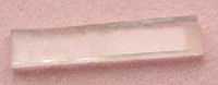
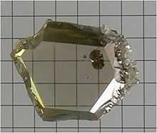
| Appearance | yellow powder |
| Density | 6.15 g/cm3 |
| Melting point | >2500 °C[1] |
| Reacts. | |
| Band gap | 3.4 eV (300 K, direct) |
| Electron mobility | 440 cm2/(V·s) (300 K) |
| Thermal conductivity | 1.3 W/(cm·K) (300 K) [2] |
| Refractive index (nD) |
2.429 |
| Structure | |
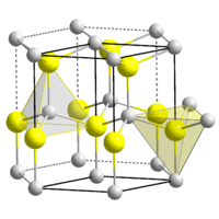
| Crystal structure | Wurtzite |
| Space group | C6v4-P63mc |
| Lattice constant | a = 3.186 Å, c = 5.186 Å [3] |
| Tetrahedral | |
| Hazards | |
| EU Index | Not listed |
| Flash point | Non-flammable |
| Related compounds | |
| Other anions |
Gallium phosphide Gallium arsenide Gallium antimonide |
| Other cations |
Boron nitride Aluminium nitride Indium nitride |
| Related compounds |
Aluminium gallium arsenide Indium gallium arsenide Gallium arsenide phosphide Aluminium gallium nitride Indium gallium nitride |
| Except where noted otherwise, data is given for materials in their standard state (at 25 °C (77 °F), 100 kPa) | |
| | |
| Infobox references | |
Gallium nitride (GaN) is a binary III/V direct bandgap semiconductor commonly used in bright light-emitting diodes since the 1990s. The compound is a very hard material that has a Wurtzite crystal structure. Its wide band gap of 3.4 eV affords it special properties for applications in optoelectronic,[4][5] high-power and high-frequency devices. For example, GaN is the substrate which makes violet (405 nm) laser diodes possible, without use of nonlinear optical frequency-doubling.
Its sensitivity to ionizing radiation is low (like other group III nitrides), making it a suitable material for solar cell arrays for satellites. Military and space applications could also benefit as devices have shown stability in radiation environments.[6] Because GaN transistors can operate at much higher temperatures and work at much higher voltages than gallium arsenide (GaAs) transistors, they make ideal power amplifiers at microwave frequencies.
Physical properties
GaN is a very hard, mechanically stable wide bandgap semiconductor material with high heat capacity and thermal conductivity.[7] In its pure form it resists cracking and can be deposited in thin film on sapphire or silicon carbide, despite the mismatch in their lattice constants.[7] GaN can be doped with silicon (Si) or with oxygen[8] to n-type and with magnesium (Mg) to p-type;[9] however, the Si and Mg atoms change the way the GaN crystals grow, introducing tensile stresses and making them brittle.[10] Gallium nitride compounds also tend to have a high spatial defect frequency, on the order of a hundred million to ten billion defects per square centimeter.[11]
Developments
GaN with a high crystalline quality can be obtained by depositing a buffer layer at low temperatures.[12] Such high-quality GaN led to the discovery of p-type GaN,[9] p-n junction blue/UV-LEDs[9] and room-temperature stimulated emission[13] (indispensable for laser action).[14] This has led to the commercialization of high-performance blue LEDs and long-lifetime violet-laser diodes, and to the development of nitride-based devices such as UV detectors and high-speed field-effect transistors.
High-brightness GaN light-emitting diodes (LEDs) completed the range of primary colors, and made applications such as daylight visible full-color LED displays, white LEDs and blue laser devices possible. The first GaN-based high-brightness LEDs were using a thin film of GaN deposited via MOCVD on sapphire. Other substrates used are zinc oxide, with lattice constant mismatch only 2%, and silicon carbide (SiC).[15] Group III nitride semiconductors are in general recognized as one of the most promising semiconductor family for fabricating optical devices in the visible short-wavelength and UV region.
The very high breakdown voltages,[16] high electron mobility and saturation velocity of GaN has also made it an ideal candidate for high-power and high-temperature microwave applications, as evidenced by its high Johnson's Figure of Merit. Potential markets for high-power/high-frequency devices based on GaN include microwave radio-frequency power amplifiers (such as used in high-speed wireless data transmission) and high-voltage switching devices for power grids. A potential mass-market application for GaN-based RF transistors is as the microwave source for microwave ovens, replacing the magnetrons currently used. The large band gap means that the performance of GaN transistors is maintained up to higher temperatures than silicon transistors. The first gallium nitride metal semiconductor field-effect transistors (GaN MESFET) were experimentally demonstrated in 1993[17] and they are being actively developed.
In 2010 the first enhancement mode gallium nitride transistors became generally available.[18] These devices were designed to replace power MOSFETs in applications where switching speed or power conversion efficiency is critical. These transistors, also called eGaN FETs, are built by growing a thin layer of GaN on top of a standard silicon wafer. This allows the eGaN FETs to maintain costs similar to silicon power MOSFETs, but with the superior electrical performance GaN.
Applications
GaN-based violet laser diodes are used to read Blu-ray Discs. When doped with a suitable transition metal such as manganese, GaN is a promising spintronics material (magnetic semiconductors). The mixture of GaN with In (InGaN) or Al (AlGaN) with a band gap dependent on ratio of In or Al to GaN allows the manufacture of light-emitting diodes (LEDs) with colors that can go from red to ultra-violet.[15]
GaN HEMTs have been offered commercially since 2006, and have found immediate use in various wireless infrastructure applications due to their high efficiency and high voltage operation. Second generation technology with shorter gate lengths will be addressing higher frequency telecom and aerospace applications.[19] GaN based MOSFET and MESFET transistors also offer many advantages in high power electronics, especially in automotive and electric car applications.[20] Nanotubes of GaN are proposed for applications in nanoscale electronics, optoelectronics and biochemical-sensing applications[21]
They are also useful in military electronics such as active electronically scanned array radars.[22]
SAAB´s JAS 39 Gripen NG (E and F variant) is using an electronic warfare system based on gallium nitride technology.[23]
Synthesis
Bulk substrates
GaN crystals can be grown from a molten Na/Ga melt held under 100 atm pressure of N2 at 750 °C. As Ga will not react with N2 below 1000 °C, the powder must be made from something more reactive, usually in one of the following ways:
- 2 Ga + 2 NH3 → 2 GaN + 3 H2
- Ga2O3 + 2 NH3 → 2 GaN + 3 H2O
Molecular beam epitaxy
Commercially, GaN crystals can be grown using molecular beam epitaxy. This process can be further modified to reduce dislocation densities. First, an ion beam is applied to the growth surface in order to create nanoscale roughness. Then, the surface is polished. This process takes place in a vacuum.
Safety
GaN dust is an irritant to skin, eyes and lungs. The environment, health and safety aspects of gallium nitride sources (such as trimethylgallium and ammonia) and industrial hygiene monitoring studies of MOVPE sources have been reported recently in a review.[24]
Bulk GaN is non-toxic and biocompatible,[25] and therefore may be used in the electrodes and electronics of implants in living organisms.
See also
- Schottky diode
- Semiconductor devices
- Molecular-beam epitaxy
- Epitaxy
References
- ↑ Harafuji, Kenji; Tsuchiya, Taku; Kawamura, Katsuyuki (2004). "Molecular dynamics simulation for evaluating melting point of wurtzite-type GaN crystal". Appl. Phys. 96 (5): 2501. Bibcode:2004JAP....96.2501H. doi:10.1063/1.1772878.
- ↑ Mion, Christian (2005). "Investigation of the Thermal Properties of Gallium Nitride Using the Three Omega Technique", Thesis, North Carolina State University.
- ↑ Bougrov V., Levinshtein M.E., Rumyantsev S.L., Zubrilov A., in Properties of Advanced Semiconductor Materials GaN, AlN, InN, BN, SiC, SiGe. Eds. Levinshtein M.E., Rumyantsev S.L., Shur M.S., John Wiley & Sons, Inc., New York, 2001, 1–30
- ↑ Di Carlo, A. (2001). "Tuning Optical Properties of GaN-Based Nanostructures by Charge Screening". Physica status solidi (a) 183: 81. Bibcode:2001PSSAR.183...81D. doi:10.1002/1521-396X(200101)183:1<81::AID-PSSA81>3.0.CO;2-N.
- ↑ Arakawa, Y. (2002). "Progress in GaN-based quantum dots for optoelectronics applications". IEEE Journal of Selected Topics in Quantum Electronics 8 (4): 823–832. doi:10.1109/JSTQE.2002.801675.
- ↑ Lidow, Alexander; Witcher, J. Brandon and Smalley, Ken (March 2011). "Enhancement Mode Gallium Nitride (eGaN) FET Characteristics under Long Term Stress" (PDF). GOMAC Tech Conference.
- ↑ 7.0 7.1 Akasaki, I.; Amano, H. (1997). "Crystal Growth and Conductivity Control of Group III Nitride Semiconductors and Their Application to Short Wavelength Light Emitters". Japanese Journal of Applied Physics 36: 5393. doi:10.1143/JJAP.36.5393.
- ↑ Wetzel, C.; Suski, T.; Ager, J.W. III; Fischer, S.; Meyer, B.K.; Grzegory, I.; Porowski, S. (1996) Strongly localized donor level in oxygen doped gallium nitride, International conference on physics of semiconductors, Berlin (Germany), 21–26 July 1996.
- ↑ 9.0 9.1 9.2 Amano, H.; Kito, M.; Hiramatsu, K.; Akasaki, I. (1989). "P-Type Conduction in Mg-Doped GaN Treated with Low-Energy Electron Beam Irradiation (LEEBI)". Japanese Journal of Applied Physics 28: L2112. doi:10.1143/JJAP.28.L2112.
- ↑ Terao, S.; Iwaya, M.; Nakamura, R.; Kamiyama, S.; Amano, H.; Akasaki, I. (2001). "Fracture of AlxGa1-xN/GaN Heterostructure – Compositional and Impurity Dependence –". Japanese Journal of Applied Physics 40: L195. Bibcode:2001JaJAP..40..195T. doi:10.1143/JJAP.40.L195.
- ↑ Preuss, Paul (11 August 2000). Blue Diode Research Hastens Day of Large-Scale Solid-State Light Sources. Berkeley Lab., lbl.gov.
- ↑ Amano, H.; Sawaki, N.; Akasaki, I.; Toyoda, Y. (1986). "Metalorganic vapor phase epitaxial growth of a high quality GaN film using an AlN buffer layer". Applied Physics Letters 48 (5): 353. Bibcode:1986ApPhL..48..353A. doi:10.1063/1.96549.
- ↑ Amano, H.; Asahi, T.; Akasaki, I. (1990). "Stimulated Emission Near Ultraviolet at Room Temperature from a GaN Film Grown on Sapphire by MOVPE Using an AlN Buffer Layer". Japanese Journal of Applied Physics 29: L205. doi:10.1143/JJAP.29.L205.
- ↑ Akasaki, I.; Amano, H.; Sota, S.; Sakai, H.; Tanaka, T.; Masayoshikoike (1995). "Stimulated Emission by Current Injection from an AlGaN/GaN/GaInN Quantum Well Device". Japanese Journal of Applied Physics 34: L1517. doi:10.1143/JJAP.34.L1517.
- ↑ 15.0 15.1 Morkoç, H.; Strite, S.; Gao, G. B.; Lin, M. E.; Sverdlov, B.; Burns, M. (1994). "Large-band-gap SiC, III-V nitride, and II-VI ZnSe-based semiconductor device technologies". Journal of Applied Physics 76 (3): 1363. Bibcode:1994JAP....76.1363M. doi:10.1063/1.358463.
- ↑ Dora, Y.; Chakraborty, A.; McCarthy, L.; Keller, S.; Denbaars, S. P.; Mishra, U. K. (2006). "High Breakdown Voltage Achieved on AlGaN/GaN HEMTs with Integrated Slant Field Plates". IEEE Electron Device Letters 27 (9): 713. doi:10.1109/LED.2006.881020.
- ↑ Asif Khan, M.; Kuznia, J. N.; Bhattarai, A. R.; Olson, D. T. (1993). "Metal semiconductor field effect transistor based on single crystal GaN". Applied Physics Letters 62 (15): 1786. Bibcode:1993ApPhL..62.1786A. doi:10.1063/1.109549.
- ↑ Davis, Sam (March 2010). "Enhancement Mode GaN MOSFET Delivers Impressive Performance". Power Electronic Technology 36 (3).
- ↑ 2010 IEEE Intl. Symposium, Technical Abstract Book, Session TH3D, pp. 164–165
- ↑ SiC and GaN Vie for Slice of the Electric Vehicle Pie. Powerelectronics. November 1, 2009
- ↑ Goldberger, J.; He, R.; Zhang, Y.; Lee, S.; Yan, H.; Choi, H. J.; Yang, P. (2003). "Single-crystal gallium nitride nanotubes". Nature 422 (6932): 599–602. doi:10.1038/nature01551. PMID 12686996.
- ↑ "Gallium Nitride-Based Modules Set New 180-Day Standard For High Power Operation." Northrop Grumman, 13 April 2011.
- ↑ The Planet’s Best Stealth Fighter Isn’t Made in America. The Daily Beast. 24 March 2014.
- ↑ Shenai-Khatkhate, D. V.; Goyette, R. J.; Dicarlo, R. L. Jr; Dripps, G. (2004). "Environment, health and safety issues for sources used in MOVPE growth of compound semiconductors". Journal of Crystal Growth 272 (1–4): 816–21. Bibcode:2004JCrGr.272..816S. doi:10.1016/j.jcrysgro.2004.09.007.
- ↑ Shipman, Matt and Ivanisevic, Albena (24 October 2011). "Research Finds Gallium Nitride is Non-Toxic, Biocompatible – Holds Promise For Biomedical Implants". North Carolina State University
External links
| Wikimedia Commons has media related to Gallium nitride. |
| ||||||