Equivalent impedance transforms
| Linear network analysis | |
|---|---|
| Elements | |
| Components | |
| Series and parallel circuits | |
|
| |
| Impedance transforms | |
| Generator theorems | Network theorems |
| Network analysis methods | |
| Two-port parameters | |
An equivalent impedance is an equivalent circuit of an electrical network of impedance elements[note 2] which presents the same impedance between all pairs of terminals[note 10] as did the given network. This article describes mathematical transformations between some passive, linear impedance networks commonly found in electronic circuits.
There are a number of very well known and often used equivalent circuits in linear network analysis. These include resistors in series, resistors in parallel and the extension to series and parallel circuits for capacitors, inductors and general impedances. Also well known are the Norton and Thévenin equivalent current generator and voltage generator circuits respectively, as is the Y-Δ transform. None of these are discussed in detail here; the individual linked articles should be consulted.
The number of equivalent circuits that a linear network can be transformed into is unbounded. Even in the most trivial cases this can be seen to be true, for instance, by asking how many different combinations of resistors in parallel are equivalent to a given combined resistor. The number of series and parallel combinations that can be formed grows exponentially with the number of resistors, n. For large n the size of the set has been found by numerical techniques to be approximately 2.53n and analytically strict bounds are given by a Farey sequence of Fibonacci numbers.[1] This article could never hope to be comprehensive, but there are some generalisations possible. Wilhelm Cauer found a transformation that could generate all possible equivalents of a given rational,[note 9] passive, linear one-port,[note 8] or in other words, any given two-terminal impedance. Transformations of 4-terminal, especially 2-port, networks are also commonly found and transformations of yet more complex networks are possible.
The vast scale of the topic of equivalent circuits is underscored in a story told by Sidney Darlington. According to Darlington, a large number of equivalent circuits were found by Ronald Foster, following his and George Campbell's 1920 paper on non-dissipative four-ports. In the course of this work they looked at the ways four ports could be interconnected with ideal transformers[note 5] and maximum power transfer. They found a number of combinations which might have practical applications and asked the AT&T patent department to have them patented. The patent department replied that it was pointless just patenting some of the circuits if a competitor could use an equivalent circuit to get around the patent; they should patent all of them or not bother. Foster therefore set to work calculating every last one of them. He arrived at an enormous total of 83,539 equivalents (577,722 if different output ratios are included). This was too many to patent, so instead the information was released into the public domain in order to prevent any of AT&T's competitors from patenting them in the future.[2][3]
2-terminal, 2-element-kind networks
A single impedance has two terminals to connect to the outside world, hence can be described as a 2-terminal, or a one-port, network. Despite the simple description, there is no limit to the number of meshes,[note 6] and hence complexity and number of elements, that the impedance network may have. 2-element-kind[note 4] networks are common in circuit design; filters, for instance, are often LC-kind networks and printed circuit designers favour RC-kind networks because inductors are less easy to manufacture. Transformations are simpler and easier to find than for 3-element-kind networks. One-element-kind networks can be thought of as a special case of two-element-kind. It is possible to use the transformations in this section on a certain few 3-element-kind networks by substituting a network of elements for element Zn. However, this is limited to a maximum of two impedances being substituted; the remainder will not be a free choice. All the transformation equations given in this section are due to Otto Zobel.[4]
3-element networks
One-element networks are trivial and two-element,[note 3] two-terminal networks are either two elements in series or two elements in parallel, also trivial. The smallest number of elements that is non-trivial is three, and there are two 2-element-kind non-trivial transformations possible, one being both the reverse transformation and the topological dual, of the other.[5]
| Description | Network | Transform equations | Transformed network |
|---|---|---|---|
| Transform 1.1 Transform 1.2 is the reverse of this transform. |
.svg.png) |
   |
.svg.png) |
| Transform 1.2 The reverse transform, and topological dual, of Transform 1.1. |
.svg.png) |
   |
.svg.png) |
| Example 1. An example of Transform 1.2. The reduced size of the inductor has practical advantages. |
.svg.png) |
    |
.svg.png) |
4-element networks
There are four non-trivial 4-element transformations for 2-element-kind networks. Two of these are the reverse transformations of the other two and two are the dual of a different two. Further transformations are possible in the special case of Z2 being made the same element kind as Z1, that is, when the network is reduced to one-element-kind. The number of possible networks continues to grow as the number of elements is increased. For all entries in the following table it is defined:[6]
|
|
| Description | Network | Transform equations | Transformed network |
|---|---|---|---|
| Transform 2.1 Transform 2.2 is the reverse of this transform. Transform 2.3 is the topological dual of this transform. |
.svg.png) |
    |
.svg.png) |
| Transform 2.2 Transform 2.1 is the reverse of this transform. Transform 2.4 is the topological dual of this transform. |
.svg.png) |
    |
.svg.png) |
| Transform 2.3 Transform 2.4 is the reverse of this transform. Transform 2.1 is the topological dual of this transform. |
.svg.png) |
    |
.svg.png) |
| Transform 2.4 Transform 2.3 is the reverse of this transform. Transform 2.2 is the topological dual of this transform. |
.svg.png) |
    |
.svg.png) |
| Example 2. An example of Transform 2.2. |
.svg.png) |
       |
.svg.png) |
2-terminal, n-element, 3-element-kind networks

Simple networks with just a few elements can be dealt with by formulating the network equations "by hand" with the application of simple network theorems such as Kirchhoff's laws. Equivalence is proved between two networks by directly comparing the two sets of equations and equating coefficients. For large networks more powerful techniques are required. A common approach is to start by expressing the network of impedances as a matrix. This approach is only good for rational[note 9] networks. Any network that includes distributed elements, such as a transmission line, cannot be represented by a finite matrix. Generally, an n-mesh[note 6] network requires an nxn matrix to represent it. For instance the matrix for a 3-mesh network might look like;
The entries of the matrix are chosen so that the matrix forms a system of linear equations in the mesh voltages and currents (as defined for mesh analysis);
The example diagram in Figure 1, for instance, can be represented as an impedance matrix by;
and the associated system of linear equations are,
In the most general case, each branch,[note 1] Zp, of the network may be made up of three elements so that,

- where L, R and C represent inductance, resistance, and capacitance respectively and s is the complex frequency operator
 .
.
This is the conventional way of representing a general impedance but for the purposes of this article it is mathematically more convenient to deal with elastance, D, the inverse of capacitance, C. In those terms the general branch impedance can be represented by,
Likewise, each entry of the impedance matrix can consist of the sum of three elements. Consequently, the matrix can be decomposed into three nxn matrices, one for each of the three element kinds;
It is desired that the matrix [Z] represent an impedance, Z(s). For this purpose, the loop of one of the meshes is cut and Z(s) is the impedance measured between the points so cut. It is conventional to assume the external connection port is in mesh 1, and is therefore connected across matrix entry Z11, although it would be perfectly possible to formulate this with connections to any desired nodes.[note 7] In the following discussion Z(s) taken across Z11 is assumed. Z(s) may be calculated from [Z] by;[7]

- where z11 is the complement of Z11 and |Z| is the determinant of [Z].
For the example network above;

 and,
and,
This result is easily verified to be correct by the more direct method of resistors in series and parallel. However, such methods rapidly become tedious and cumbersome with the growth of the size and complexity of the network under analysis.
The entries of [R], [L] and [D] cannot be set arbitrarily. For [Z] to be able to realise the impedance Z(s) then [R],[L] and [D] must all be positive-definite matrices. Even then, the realisation of Z(s) will, in general, contain ideal transformers[note 5] within the network. Finding only those transforms that do not require mutual inductances or ideal transformers is a more difficult task. Similarly, if starting from the "other end" and specifying an expression for Z(s), this again cannot be done arbitrarily. To be realisable as a rational impedance, Z(s) must be positive-real. The positive-real (PR) condition is both necessary and sufficient[8] but there may be practical reasons for rejecting some topologies.[7]
A general impedance transform for finding equivalent rational one-ports from a given instance of [Z] is due to Wilhelm Cauer. The group of real affine transformations,
- where,
![\mathbf{[T]}=\begin{bmatrix} 1 & 0 \cdots 0 \\ T_{21} & T_{22} \cdots T_{2n} \\ \cdot & \cdots \\ T_{n1} & T_{n2} \cdots T_{nn}\end{bmatrix}](../I/m/536c654498178be01c80848fde1b6ba5.png)
is invariant in Z(s). That is, all the transformed networks are equivalents according to the definition given here. If the Z(s) for the initial given matrix is realisable, that is, it meets the PR condition, then all the transformed networks produced by this transformation will also meet the PR condition.[7]
3 and 4-terminal networks

When discussing 4-terminal networks, network analysis often proceeds in terms of 2-port networks, which covers a vast array of practically useful circuits. "2-port", in essence, refers to the way the network has been connected to the outside world: that the terminals have been connected in pairs to a source or load. It is possible to take exactly the same network and connect it to external circuitry in such a way that it is no longer behaving as a 2-port. This idea is demonstrated in Figure 2.
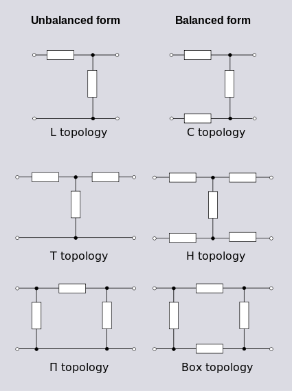
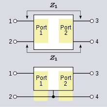
A 3-terminal network can also be used as a 2-port. To achieve this, one of the terminals is connected in common to one terminal of both ports. In other words, one terminal has been split into two terminals and the network has effectively been converted to a 4-terminal network. This topology is known as unbalanced topology and is opposed to balanced topology. Balanced topology requires, referring to Figure 3, that the impedance measured between terminals 1 and 3 is equal to the impedance measured between 2 and 4. This is the pairs of terminals not forming ports: the case where the pairs of terminals forming ports have equal impedance is referred to as symmetrical. Strictly speaking, any network that does not meet the balance condition is unbalanced, but the term is most often referring to the 3-terminal topology described above and in Figure 3. Transforming an unbalanced 2-port network into a balanced network is usually quite straightforward: all series connected elements are divided in half with one half being relocated in what was the common branch. Transforming from balanced to unbalanced topology will often be possible with the reverse transformation but there are certain cases of certain topologies which cannot be transformed in this way. For example, see the discussion of lattice transforms below.
An example of a 3-terminal network transform that is not restricted to 2-ports is the Y-Δ transform. This is a particularly important transform for finding equivalent impedances. Its importance arises from the fact that the total impedance between two terminals cannot be determined solely by calculating series and parallel combinations except for a certain restricted class of network. In the general case additional transformations are required. The Y-Δ transform, its inverse the Δ-Y transform, and the n-terminal analogues of these two transforms (star-polygon transforms) represent the minimal additional transforms required to solve the general case. Series and parallel are, in fact, the 2-terminal versions of star and polygon topology. A common simple topology that cannot be solved by series and parallel combinations is the input impedance to a bridge network (except in the special case when the bridge is in balance).[9] The rest of the transforms in this section are all restricted to use with 2-ports only.
Lattice transforms
Symmetric 2-port networks can be transformed into lattice networks using Bartlett's bisection theorem. The method is limited to symmetric networks but this includes many topologies commonly found in filters, attenuators and equalisers. The lattice topology is intrinsically balanced, there is no unbalanced counterpart to the lattice and it will usually require more components than the transformed network.
| Some common networks transformed to lattices (X-networks) | |||
|---|---|---|---|
| Description | Network | Transform equations | Transformed network |
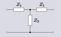
| Transform 3.1 Transform of T network to lattice network.[10] |
 |
  |
 |
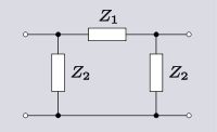
| Transform 3.2 Transform of Π network to lattice network.[10] |
 |
  |
 |
| Transform 3.3 Transform of Bridged-T network to lattice network.[11] |
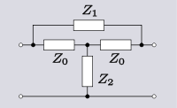 |
  |
 |
Reverse transformations from a lattice to an unbalanced topology are not always possible in terms of passive components. For instance, this transform,
| Description | Network | Transformed network |
|---|---|---|
| Transform 3.4 Transform of a lattice phase equaliser to a T network.[12] |
 |
 |
cannot be realised with passive components because of the negative values arising in the transformed circuit. It can however be realised if mutual inductances and ideal transformers are permitted, for instance, in this circuit. Another possibility is to permit the use of active components which would enable negative impedances to be directly realised as circuit components.[13]
It can sometimes be useful to make such a transformation, not for the purposes of actually building the transformed circuit, but rather, for the purposes of aiding understanding of how the original circuit is working. The following circuit in bridged-T topology is a modification of a mid-series m-derived filter T-section. The circuit is due to Hendrik Bode who claims that the addition of the bridging resistor of a suitable value will cancel the parasitic resistance of the shunt inductor. The action of this circuit is clear if it is transformed into T topology - in this form there is a negative resistance in the shunt branch which can be made to be exactly equal to the positive parasitic resistance of the inductor.[14]
| Description | Network | Transformed network |
|---|---|---|
| Transform 3.5 Transform of a bridged-T low-pass filter section to a T-section.[14] |
 |
 |
Any symmetrical network can be transformed into any other symmetrical network by the same method, that is, by first transforming into the intermediate lattice form (omitted for clarity from the above example transform) and from the lattice form into the required target form. As with the example, this will generally result in negative elements except in special cases.[15]
Eliminating resistors
A theorem due to Sidney Darlington states that any PR function Z(s) can be realised as a lossless two-port terminated in a positive resistor R. That is, regardless of how many resistors feature in the matrix [Z] representing the impedance network, a transform can be found that will realise the network entirely as an LC-kind network with just one resistor across the output port (which would normally represent the load). No resistors within the network are necessary in order to realise the specified response. Consequently, it is always possible to reduce 3-element-kind 2-port networks to 2-element-kind (LC) 2-port networks provided the output port is terminated in a resistance of the required value.[8][16][17]
Eliminating ideal transformers
An elementary transformation that can be done with ideal transformers and some other impedance element is to shift the impedance to the other side of the transformer. In all the following transforms, r is the turns ratio of the transformer.
| Description | Network | Transformed network |
|---|---|---|
| Transform 4.1 Series impedance through a step-down transformer. |
.svg.png) |
.svg.png) |
| Transform 4.2 Shunt impedance through a step-down transformer. |
.svg.png) |
.svg.png) |
| Transform 4.3 Shunt and series impedance network through a step-up transformer. |
.svg.png) |
.svg.png) |
These transforms do not just apply to single elements; entire networks can be passed through the transformer. In this manner, the transformer can be shifted around the network to a more convenient location.
Darlington gives an equivalent transform that can eliminate an ideal transformer altogether. This technique requires that the transformer is next to (or capable of being moved next to) an "L" network of same-kind impedances. The transform in all variants results in the "L" network facing the opposite way, that is, topologically mirrored.[2]
| Description | Network | Transformed network |
|---|---|---|
| Transform 5.1 Elimination of a step-down transformer. |
.svg.png) |
.svg.png) |
| Transform 5.2 Elimination of a step-up transformer. |
.svg.png) |
.svg.png) |
| Example 3. Example of transform 5.1. |
.svg.png) |
.svg.png) |
Example 3 shows the result is a Π-network rather than an L-network. The reason for this is that the shunt element has more capacitance than is required by the transform so some is still left over after applying the transform. If the excess were instead, in the element nearest the transformer, this could be dealt with by first shifting the excess to the other side of the transformer before carrying out the transform.[2]
Terminology
- ↑ 1.0 1.1 Branch. A network branch is a group of elements connected in series between two nodes. An essential feature of a branch is that all elements in the branch have the same current flowing through them.
- ↑ 2.0 2.1 Element. A component in a network, an individual resistor (R), inductor (L) or capacitor (C).
- ↑ 3.0 3.1 n-element. A network that contains a total of n elements of all kinds.
- ↑ 4.0 4.1 n-element-kind. A network that contains n different kinds of elements. For instance, a network consisting solely of LC elements is a 2-element-kind network.
- ↑ 5.0 5.1 5.2 Ideal transformer. These frequently appear in network analysis. They are a purely theoretical construct which perfectly transform voltages and currents by the given ratio without loss. Real transformers are highly efficient and can often be used in place of an ideal transformer. One essential difference is that ideal transformers continue to work when energised with DC, something no real transformer could ever do. See transformer.
- ↑ 6.0 6.1 6.2 n-mesh. A mesh is a loop of a network where connections exist to allow current to pass from element to element, and form an unbroken path returning eventually to the starting point. An essential mesh is such a loop that does not contain any other loop. An n-mesh network is one that contains n essential meshes.
- ↑ 7.0 7.1 Node. A network node is point in a circuit where one terminal of three or more elements are joined.
- ↑ 8.0 8.1 Port. A pair of terminals of a network into which flows equal and opposite currents.
- ↑ 9.0 9.1 9.2 Rational in this context means a network composed of a finite number of elements. Distributed elements, such as in a transmission line, are therefore excluded because the infinitessimal nature of the elements will cause their number to go to infinity.
- ↑ 10.0 10.1 Terminal. A point in a network to which voltages external to the network can be connected and into which external currents may flow. A 2-terminal network is also a one-port network. 3-terminal and 4-terminal networks are often, but not always, also connected as 2-port networks.
References
- ↑ Khan, p.154
- ↑ 2.0 2.1 2.2 Darlington, p.6.
- ↑ Foster and Campbell, p.233
- ↑ Zobel, 1923.
- ↑ Zobel, p.45.
- ↑ Zobel, pp.45-46.
- ↑ 7.0 7.1 7.2 E. Cauer et al., p.4.
- ↑ 8.0 8.1 Belevitch, p.850
- ↑ Farago, pp.18-21.
- ↑ 10.0 10.1 Zobel, pp.19-20.
- ↑ Farago, pp.117-121.
- ↑ Farago, p.117.
- ↑ Darlington, pp.5-6.
- ↑ 14.0 14.1 Bode, Hendrik W., Wave Filter, US patent 2 002 216, filed 7 June 1933, issued 21 May 1935.
- ↑ Bartlett, p.902.
- ↑ E. Cauer et al., pp.6–7.
- ↑ Darlington, p.7.
Bibliography
- Bartlett, A. C., "An extension of a property of artificial lines", Phil. Mag., vol 4, p.902, November 1927.
- Belevitch, V., "Summary of the history of circuit theory", Proceedings of the IRE, vol 50, Iss 5, pp.848-855, May 1962.
- E. Cauer, W. Mathis, and R. Pauli, "Life and Work of Wilhelm Cauer (1900 – 1945)", Proceedings of the Fourteenth International Symposium of Mathematical Theory of Networks and Systems, Perpignan, June, 2000.
- Foster, Ronald M.; Campbell, George A., "Maximum output networks for telephone substation and repeater circuits", Transactions of the American Institute of Electrical Engineers, vol.39, iss.1, pp.230-290, January 1920.
- Darlington, S., "A history of network synthesis and filter theory for circuits composed of resistors, inductors, and capacitors", IEEE Trans. Circuits and Systems, vol 31, pp.3-13, 1984.
- Farago, P. S., An Introduction to Linear Network Analysis, The English Universities Press Ltd, 1961.
- Khan, Sameen Ahmed, "Farey sequences and resistor networks", Proceedings of the Indian Academy of Sciences (Mathematical Sciences), vol.122, iss.2, pp. 153-162, May 2012.
- Zobel, O. J.,Theory and Design of Uniform and Composite Electric Wave Filters, Bell Systems Technical Journal, Vol. 2 (1923), pp.1-46.
 ,
, ,
, ,
, ,
, .
.![\mathbf{[Z]}=\begin{bmatrix} Z_{11} & Z_{12} & Z_{13} \\ Z_{21} & Z_{22} & Z_{23} \\ Z_{31} & Z_{32} & Z_{33} \end{bmatrix}](../I/m/406d9ef2156dc63caacc43c0c2e42cba.png)
![\mathbf{[V]}= \mathbf{[Z][I]}](../I/m/8137eed9d2b8dbf49a2b82592fa3a015.png)
![\mathbf{[Z]}=\begin{bmatrix} R_1+R_2 & -R_2 \\ -R_2 & R_2+R_3 \end{bmatrix}](../I/m/cc81e565e911ab1d18c833a027ac1462.png)


![s \mathbf{[Z]}= s^2 \mathbf{[L]} + s \mathbf{[R]} + \mathbf{[D]}](../I/m/7e24fe44eadc41f36b335a74091ed2b6.png)
![\mathbf{[Z']} = \mathbf{[T]}^T \mathbf{[Z]} \mathbf{[T]}](../I/m/ff2ffdfb7a5eab4f445cd66f87dc9dd2.png)