Early effect
.svg)
The Early effect is the variation in the width of the base in a bipolar junction transistor (BJT) due to a variation in the applied base-to-collector voltage, named after its discoverer James M. Early. A greater reverse bias across the collector–base junction, for example, increases the collector–base depletion width, decreasing the width of the charge neutral portion of the base.
In Figure 1 the neutral (i.e. active) base is green, and the depleted base regions are hashed light green. The neutral emitter and collector regions are dark blue and the depleted regions hashed light blue. Under increased collector–base reverse bias, the lower panel of Figure 1 shows a widening of the depletion region in the base and the associated narrowing of the neutral base region.
The collector depletion region also increases under reverse bias, more than does that of the base, because the collector is less heavily doped. The principle governing these two widths is charge neutrality. The narrowing of the collector does not have a significant effect as the collector is much longer than the base. The emitter–base junction is unchanged because the emitter–base voltage is the same.
.svg)
Base-narrowing has two consequences that affect the current:
- There is a lesser chance for recombination within the "smaller" base region.
- The charge gradient is increased across the base, and consequently, the current of minority carriers injected across the emitter junction increases.
Both these factors increase the collector or "output" current of the transistor with an increase in the collector voltage. This increased current is shown in Figure 2. Tangents to the characteristics at large voltages extrapolate backward to intercept the voltage axis at a voltage called the Early voltage, often denoted by the symbol VA.
Large-signal model
In the forward active region the Early effect modifies the collector current ( ) and the forward common-emitter current gain (
 ), as typically described by the following equations:[1][2]
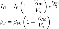
Where
-
 is the collector–emitter voltage
 -
 is the thermal voltage
  ; see thermal voltage: role in semiconductor physics
 -
 is the Early voltage (typically 15 V to 150 V; smaller for smaller devices)
 -
 is forward common-emitter current gain at zero bias.
Some models base the collector current correction factor on the collector–base voltage VCB (as described in base-width modulation) instead of the collector–emitter voltage VCE.[3] Using VCB may be more physically plausible, in agreement with the physical origin of the effect, which is a widening of the collector–base depletion layer that depends on VCB. Computer models such as those used in SPICE use the collector–base voltage VCB.[4]
Small-signal model
The Early effect can be accounted for in small-signal circuit models (such as the hybrid-pi model) as a resistor defined as[5]
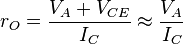
in parallel with the collector–emitter junction of the transistor. This resistor can thus account for the finite output resistance of a simple current mirror or an actively loaded common-emitter amplifier.
In keeping with the model used in SPICE and as discussed above using  the resistance becomes:
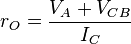
which almost agrees with the textbook result. In either formulation,  varies with DC reverse bias , as is observed in practice.
In the MOSFET the output resistance is given in Shichman–Hodges model[6] (accurate for very old technology) as:
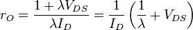
where  = drain-to-source voltage,
  = drain current and
  = channel-length modulation parameter, usually taken as inversely proportional to channel length L.
Because of the resemblance to the bipolar result, the terminology "Early effect" often is applied to the MOSFET as well.
= channel-length modulation parameter, usually taken as inversely proportional to channel length L.
Because of the resemblance to the bipolar result, the terminology "Early effect" often is applied to the MOSFET as well.
Current–voltage characteristics
The expressions are derived for a PNP transistor. For an NPN transistor, n has to be replaced by p, and p has to be replaced by n in all expressions below. The following assumptions are involved when deriving ideal current-voltage characteristics of the BJT[7]
- Low level injection
- Uniform doping in each region with abrupt junctions
- One-dimensional current
- Negligible recombination-generation in space charge regions
- Negligible electric fields outside of space charge regions.
It is important to characterize the minority diffusion currents induced by injection of carriers.
With regard to pn-junction diode, a key relation is the diffusion equation.
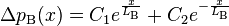
A solution of this equation is below, and two boundary conditions are used to solve and find  and
and  .
.
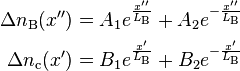
The following equations apply to the emitter and collector region, respectively, and the origins  ,
,  , and
, and  apply to the base, collector, and emitter.
A boundary condition of the emitter is below:
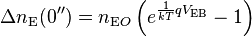
The values of the constants  and
and  are zero due to the following conditions of the emitter and collector regions as
  and
and  .
.
Because  , the values of
  and
and  are
are  and
and  , respectively.
Expressions of  and
and  can be evaluated.
Because insignificant recombination occurs, the second derivative of  is zero. There is therefore a linear relationship between excess hole density and
  .
.
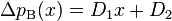
The following are boundary conditions of  .
.
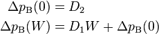
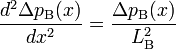
with W the base width. Substitute into the above linear relation.
![\Delta p_\text{B}(x) = -\frac{1}{W}\left[\Delta p_\text{B}(0) - \Delta p_\text{B}(W)\right]x + \Delta p_\text{B}(0)](../I/m/5d8123759225c0685cb401308d760a8a.png)
With this result, derive value of  .
.
![\begin{align}
I_{\text{E}p} (0) &= -q A D_{\text{B}} \frac{d \Delta p_\text{B}}{dx}|_{x=0} \\
I_{\text{E}p} (0) &= \frac{q A D_\text{B}}{W} \left[\Delta p_\text{B}(0) - \Delta p_\text{B}(W)\right]
\end{align}](../I/m/27476690d3fb63d9aed62e3cb559d90e.png)
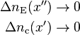
Use the expressions of , ,  , and
, and  to develop an expression of the emitter current.
![\begin{align}
\Delta p_{\text{B}}(W) &= p_{\text{B}0} e^{\frac{q V_\text{CB}}{kT}} \\
\Delta p_{\text{B}}(0) &= p_{\text{B}0} e^{\frac{q V_\text{EB}}{kT}} \\
I_{\text{E}} &= qA \left[ \left(\frac{D_\text{E} n_{\text{E}0}}{L_\text{E}} + \frac{D_\text{B} p_{\text{B}0}}{W}\right)
\left(e^{\frac{q V_\text{EB}}{kT}} - 1 \right) -
\frac{D_{\text{B}}}{W} p_{\text{B}0}\left( e^{\frac{q V_{\text{CB}}}{k T}} - 1 \right)
\right]
\end{align}](../I/m/68174407f5112628e83f8699c88116b5.png)
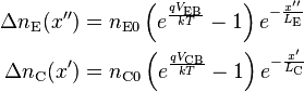
Similarly, an expression of the collector current is derived.
![\begin{align}
I_{\text{C}p}(W) &= I_{\text{E}p}(0) \\
I_{\text{C}} &= I_{\text{C}p}(W) + I_{\text{C}n}(0') \\
I_{\text{C}} &= q A \left[ \frac{D_\text{B}}{W} p_{\text{B}0}\left(e^{\frac{q V_\text{EB}}{kT}} - 1\right) -
\left(\frac{D_\text{C} n_{\text{C}0}}{L_\text{C}} + \frac{D_\text{B} p_{\text{B}0}}{W}\right)
\left(e^{\frac{q V_\text{CB}}{kT}} - 1\right)
\right]
\end{align}](../I/m/a22af7a3a13be71e0530849bb5dcef2d.png)
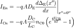
An expression of the base current is found with the previous results.
![\begin{align}
I_{\text{B}} &= I_{\text{E}} - I_{\text{C}} \\
I_{\text{B}} &= q A \left[ \frac{D_\text{E}}{L_\text{E}} n_{\text{E}0}\left(e^{\frac{q V_\text{EB}}{kT}} - 1\right) + \frac{D_\text{C}}{L_\text{C}} n_{\text{C}0}\left(e^{\frac{q V_\text{CB}}{kT}} - 1\right) \right]
\end{align}](../I/m/4dc12bc52f9f9987f37235265eb171c0.png)
References and notes
- ↑ R.C. Jaeger and T.N. Blalock (2004). Microelectronic Circuit Design. McGraw-Hill Professional. p. 317. ISBN 0-07-250503-6.
- ↑ Massimo Alioto and Gaetano Palumbo (2005). Model and Design of Bipolar and Mos Current-Mode Logic: CML, ECL and SCL Digital Circuits. Springer. ISBN 1-4020-2878-4.
- ↑ Paolo Antognetti and Giuseppe Massobrio (1993). Semiconductor Device Modeling with Spice. McGraw-Hill Professional. ISBN 0-07-134955-3.
- ↑ Orcad PSpice Reference Manual named PSpcRef.pdf, p. 209. This manual is included with the free version of Orcad PSpice, but they do not maintain a copy on line. If the link given here expires, try Googling PSpcRef.pdf.
- ↑ R.C. Jaeger and T.N. Blalock (2004). Microelectronic Circuit Design (Second Edition ed.). McGraw-Hill Professional. pp. Eq. 13.31, p. 891. ISBN 0-07-232099-0.
- ↑ The Shichman-Hodges Enhancement MOSFET Model and SwitcherCAD III SPICE, Report NDT14-08-2007, NanoDotTek, 12 August 2007
- ↑ R S Muller, Kamins TI & Chan M (2003). Device electronics for integrated circuits (Third ed.). New York: Wiley. p. 280 ff. ISBN 0-471-59398-2.