Colleges of Nanoscale Science and Engineering at SUNY Polytechnic Institute
| Colleges of Nanoscale Science and Engineering | |
|---|---|
| Established | 2004 |
| Type | College |
Academic affiliation | State University of New York |
| Endowment | - |
| Director | Alain E. Kaloyeros, Ph.D. |
| Chief academic officer | Robert Geer, Ph.D. |
Academic staff | 50 |
| Students | 321 |
| Undergraduates | 201 |
| Postgraduates |
184 total Masters: 44 Doctoral: 138 M.D./Ph.D.: 2 |
| Location |
Albany, New York 42°41′28.37″N 73°49′58.28″W / 42.6912139°N 73.8328556°WCoordinates: 42°41′28.37″N 73°49′58.28″W / 42.6912139°N 73.8328556°W |
| Website | www.sunycnse.com |
The Colleges of Nanoscale Science and Engineering (CNSE) at the State University of New York (SUNY) Polytechnic Institute are an Albany, New York, USA based global education, research, development and technology deployment resource for nanotechnology.[1] Since its inception in 2004, CNSE has gained worldwide recognition as a leader and pioneer in nanotechnology education, innovation, and economic outreach and investment.[2]
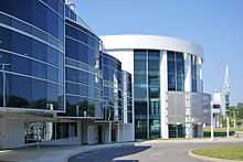
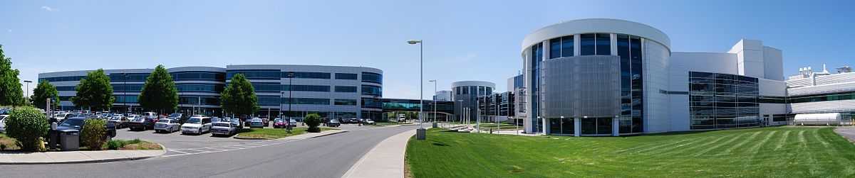
CNSE’s Albany NanoTech Complex is a $20 billion, 1,300,000-square-foot (120,000 m2) complex that includes industrial-scale 135,000-square-foot (12,500 m2) cleanroom space as well as a collection of equipment perhaps unique in the world."[3] The cleanroom space is Class 1-capable and houses a fully integrated, 300 mm and 450 mm wafer computer chip pilot prototyping and demonstration line. More than 3,100 scientists, researchers, engineers, students, and faculty work on site at CNSE’s Albany NanoTech Complex, from companies including IBM, Intel, GlobalFoundries, SEMATECH, Samsung, TSMC, Applied Materials, Tokyo Electron, ASML, and Lam Research.[4][5] CNSE’s latest expansion, which includes NanoFab Xtension (NFX), headquarters for the world’s first Global 450mm Consortium (G450C), and the Zero Energy Nanotechnology (ZEN) building, a living laboratory for green energy technologies, will add more than 1,000 scientists, researchers, and engineers from CNSE and global corporations.
History
The Colleges of Nanoscale Science and Engineering was originally established as the School of Nanosciences and Nanoengineering at the University at Albany in 2001. It began as a combined vision of government, academia, and lastly, industry. The common goal was to propel New York to a leadership position in technology and economic development. Four key drivers constituted the strategy: select an overarching discipline with ripe taxation targets(nanotechnology); invest taxpayer funds in state-of-the-art infrastructure; focus on hands-on education and training incorporating the entire supply chain; and leverage public-private partnerships.[6] CNSE was accredited as the College of Nanoscale Science and Engineering of the University at Albany in 2004, and in December of that year, awarded its first Ph.D. degrees in nanoscience.[7] In July 2013, SUNY's Board of Trustees approved a memorandum that led to the separation of CNSE from the University at Albany and includes the creation of a new degree-granting structure for the NanoCollege.[1] This was followed by the merger of the SUNY Institute of Technology (SUNYIT) with CNSE in September 2014 to create SUNY Polytechnic Institute.[8][9] In January 2015, Dr. Alain Kaloyeros was appointed by the SUNY Board of Trustees as the founding President of SUNY Poly.[10]
Academics
CNSE offers degree programs leading to the Bachelor of Science (B.S.) degree in Nanoscale Engineering and Nanoscale Science,[11] the Master of Science (M.S.) degree in either Nanoscale Science or Nanoscale Engineering, and the Doctor of Philosophy (Ph.D.) degree in either Nanoscale Science or Nanoscale Engineering. CNSE also offers a combined Masters of Science and Masters of Business Administration (M.S.-MBA) degree, the "Nano+MBA," with the ability to earn the M.S. degree in either Nanoscale Science or Nanoscale Engineering,[12] or enroll in the nanotechnology elective track while participating in UAlbany's Evening MBA program.[13] Additionally, CNSE and SUNY Downstate Medical Center offer a joint M.D. and Ph.D. program.[14] The program allows students to earn an M.D. in Medicine and a Ph.D. in Nanoscale Science or Engineering.[15] In 2010, CNSE became the first college in the U.S. to launch a comprehensive baccalaureate program in Nanoscale Engineering and Nanoscale Science.[16] Through the Spring 2013 semester, CNSE has 191 alumni.[17]
Campus
CNSE's Albany NanoTech Complex is located near Western Avenue off of Fuller Road in Albany, New York.[18] NanoFab 200 (CESTM), an earlier part of the campus, was completed June 1997. This 70,000-square-foot (6,500 m2), $16.5 million facility includes 4,000 square feet (370 m2) of cleanroom space, plus CNSE metrology labs and office space for programs such as SUNY’s Atmospheric Sciences Research Center. NanoFab South (NFS), completed March 2004, is a 150,000-square-foot (14,000 m2), $50 million facility including 32,000 square feet (3,000 m2) of 300 mm wafer, class 1-capable cleanroom space. Completed December 2005, NanoFab North (NFN) is a 230,000-square-foot (21,000 m2), $175 million facility including 35,000 square feet (3,300 m2) of cleanroom space with Class 1-capable 300mm wafer production. In March 2009, another $150 million expansion project included NanoFab East (NFE), a 250,000-square-foot (23,000 m2) office, laboratory, and classroom building, in addition to NanoFab Central (NFC), a separate 100,000-square-foot (9,300 m2) building that houses 15,000 square feet (1,400 m2) of 300mm wafer, class 1-capable cleanroom space.[19] The newest 500,000-square-foot (46,000 m2) addition to the CNSE campus consists of NanoFab Xtension (NFX), which hosts the Global 450mm Consortium as well as an additional 50,000 square feet (4,600 m2) of Class 1 capable cleanroom space, and the Zero Energy Nanotechnology (ZEN) building, a living laboratory for green energy technologies. The expansion will enable the addition of more than 1,000 scientists, researchers, and engineers from CNSE and global corporations.[19][20][21]
CNSE’s Solar Energy Development Center (SEDC), located in Halfmoon, New York, further expands CNSE’s growing portfolio of clean energy research, development, and commercialization and creates new opportunities to retain and grow New York’s high-tech, green collar workforce.[22] The 18,000-square-foot (1,700 m2) CNSE Halfmoon facility features a state-of-the-art, 100 kilowatt prototyping and demonstration line for next-generation copper indium gallium selenide (CIGS) thin film solar cells, offering critical opportunities to demonstrate emerging concepts in CIGS manufacturing, such as evaluations of innovative materials and novel processes. CNSE's SEDC also supports the U.S. Photovoltaic Manufacturing Consortium, a more than $300 million public-private collaboration headquartered at CNSE.[23]
The Smart Cities Technology Innovation Center (SCiTI), located in the landmark Kiernan Plaza in Albany, New York, will build on a strategy for "smart cities" growth and livable communities after the Capital Region Economic Development Council (CREDC) awarded CNSE $4 million taxpayer funds to support the purchase and fit-up of the site.[24] The funding will be leveraged to generate an additional $26 million in private sector support through the attraction of high-tech companies and the creation and retention of 250 high-paying jobs in downtown Albany, creating a 21st-century hub for groundbreaking research, education, and workforce training for emerging smart cities technologies, including smart devices, sensors and computer chips, integrated systems, and operating software that collect and analyze data for monitoring highway conditions and improving traffic flow; protect vital infrastructure such as bridges, data centers, and utility installations; safeguard facilities, including wastewater treatment plants; and provide e-safety and security in educational settings.[25] CNSE is initially partnering with Trinity Alliance of the Capital Region and Girls Inc. of the Greater Capital Region to develop and deliver joint nanotechnology education and workforce training programs, and with CHA, which plans to relocate its corporate headquarters and leadership team to the site.[26]
The development of the Marcy Nanocenter site in Utica, NY is led by CNSE in partnership with quasi-public Mohawk Valley EDGE to accelerate the attraction of 450mm computer chip manufacturing to the Mohawk Valley.[27] The development plan of the Marcy Nanocenter site includes up to 8.25 million square feet of teaching facilities, with up to three 450mm computer chip fabs, each with a cleanroom of approximately 450,000 square feet, a total public and private investment of $10B to $15B for each phase of development, and the creation of approximately 5,000 direct jobs and approximately 15,000 indirect jobs.[28]
The Computer Chip Commercialization Center, or QUAD-C, located in Utica, New York, and co-founded and managed by the Colleges of Nanoscale Science and Engineering, is mixed-use facility configured as headquarters of a nanotechnology partnership spearheaded by SUNY Poly that includes leading technology companies such as Advanced Nanotechnology Solutions Incorporated (ANS), SEMATECH, Atotech and CNSE partners, including IBM, Lam Research and Tokyo Electron. .[29][30] According to the Madison County Courier, the high-tech project will result in "a $125 million technology complex that leverages the same multi-faceted public-private, commercial and academic partnership approach that has proven successful at CNSE."[31] Plans call for a 250,000-square-foot (23,000 m2) facility that includes 56,000 square feet (5,200 m2) of cleanroom space. QUAD-C is already home to a number of companies, including New York-based IT enterprise nfrastructure, and VALUTEK, a manufacturer of cleanroom supplies which moved from Phoenix, Arizona.[32]
CNSE's Central New York (CNY) Hub for Emerging Nano Industries in Syracuse, NY, will specialize in providing advanced visual production research and education to support New York’s rapidly growing film and television industry, with a focus on the use of nanotechnology to drive innovations in computer-generated imagery and animation, as well as motion capture technology utilized by today’s production facilities.[33] This initiative includes a minimum private investment of $150M over seven years. SUNY Poly will provide $15M to build the facility at the Collamer Crossings Business Park in Dewitt, and Onondaga County has invested $1.4M to ensure shovel-ready status for the two 52,000 square foot buildings, offering research and development, manufacturing, and office space for a diverse cross-section of businesses, including The Film House, a California-based film and television company, which will be the facility’s first tenant.[34] As announced by Governor Cuomo in March 2014, the project will create at least 350 new high-tech jobs and 150 construction jobs.[35]
The New York Power Electronics Manufacturing Consortium, located in Rochester, NY, will invest over $500 million and create thousands of high-skilled, high-paying jobs in Upstate New York over the next five years – including at least 500 in Rochester.[36] This public-private partnership will help develop the next generation of materials used on semiconductors at State-owned R&D facilities.[37] Managed by CNSE, the development of this next generation of semiconductors will enable power devices to get smaller, faster and more efficient.[35]
The Smart System Technology & Commercialization Center of Excellence (STC), located outside of Rochester in Canandaigua, New York, was created in 2010 through a merger of two of New York State's Centers of Excellence: Infotonics Technology Center (ITC) in Canandaigua and the Center of Excellence in Nanoelectronics and Nanotechnology at CNSE, and offers state-of-the-art capabilities for MEMS fabrication and packaging at its 120,000-square-foot (11,000 m2) facility that includes 26,000 square feet (2,400 m2) of certified cleanroom space with 150mm and 200mm MEMS foundry services, complemented by a dedicated 8,000-square-foot (740 m2) MEMS and optoelectronic packaging facility.[38] The STC positions New York State as a global leader in smart system and smart device innovation and manufacturing[39][40] and also positions CNSE as a vertically integrated "one-stop-shop" for smart systems' device development and process manufacturing, coupling CNSE's preeminence in nanoelectronics R&D with ITC's expertise in integrating computer chips with hundreds of mechanical devices.[39]
The CNSE Photovoltaic Manufacturing and Technology Development Facility (CNSE MDF), to be located inside a 57,000-square-foot (5,300 m2) former Kodak building in the Canal Ponds Business Park in Rochester, New York, is part of a taxpayer-funded $100 million initiative creating the solar industry’s first full-service collaborative space dedicated to advancing crystalline silicon, technologies.[41][42][43] Further leveraging the publicly led industry-university partnership model utilized at CNSE, the CNSE MDF will include a state-of-the-art, 20,000-square-foot (1,900 m2) cleanroom instruction center and will provide a range of services and equipment, including complete manufacturing lines, access to individual tools, secure fab space for users’ proprietary tools, and pilot production services in an intellectual property (IP) secure environment.[44][45] Over $19 million in cutting-edge tools and equipment that are critical to the U.S. Department of Energy’s (DOE) SunShot initiative and which were formerly utilized by SVTC, a Silicon Valley-based solar energy company, will be relocated to the CNSE MDF to constitute the foundation of the manufacturing development line.[44][46] The CNSE MDF will also enable education and training to support the expansion of the highly skilled workforce required by the U.S. PV manufacturing industry and, in addition, will complement and expand the capabilities and expertise of the national U.S. Photovoltaic Manufacturing Consortium (PVMC), headquartered at CNSE as part of the DOE’s SunShot Initiative.[46][47]
The Buffalo Medical Innovation and Commercialization Hub, located at the Buffalo Niagara Medical Campus in Buffalo, New York, will enable a state-of-the-art, shared-user facility for research, development, and testing for drug screening, pharmaceutical development, technology optimization, business attraction, workforce training, and bioinformatics.[48] This $250 million initiative, with $200 million to be generated by private industry investment and $50 million being invested by New York State, $35 million of which will go toward new equipment and $15 million of which will go toward improving existing lab space, will support over 250 high-tech jobs on site.[49]
The Buffalo High-Tech Manufacturing Innovation Hub at RiverBend will attract and house top tier clean energy companies and enable advanced manufacturing at what will become a state-of-the art, multibillion-dollar high-tech campus.[35] SolarCity, the nation's largest solar power provider, will invest $5B to establish a one million-square-foot GigaFactory, which will produce solar panels, at the Buffalo High-Tech Manufacturing Innovation Hub at RiverBend.[50] It will be the largest facility of its kind in the Western Hemisphere, with more than 1 gigawatt of annual solar capacity when it reaches full production. More than 3,000 jobs will be created in Western New York alone and a total of nearly 5,000 jobs in the state.
The Buffalo Information Technologies Innovation and Commercialization Hub leverages a $55 million Buffalo Billion investment by the State. IBM will be the first anchor tenant in the Hub, which, in partnership with the Western New York Regional Economic Development Council (WNYREDC), State Data Center, Colleges of Nanoscale Science and Engineering (CNSE) and University at Buffalo, will train IT professionals, educate new IT staff through State University of New York (SUNY) partnerships, and develop next generation IT software needed to drive state-of-the-art discoveries in the areas of molecular research, genomics, energy efficiency development and defense. Through the Hub, IBM will bring 500 new information technology jobs to Buffalo.[51]
Constellations
The traditional departmental structure at CNSE is tailored into constellation "think-tanks" that encourage and stimulate cross-disciplinary educational curricula and research programs.[52] There are four such think-tanks. Nanoscience refers to the observation, identification, description, discovery, experimental investigation, and theoretical interpretation of nanoscale phenomena.[53] Nanoengineering is the application of nanoscience principles to practical ends, such as the design, manufacture, and operation of efficient and functional structures, machines, processes, and systems on the atomic scale.[54] Nanobioscience refers to the application of nanoscale scientific concepts and principles to the study of biological and biomedical structures and systems.[55] Nanoeconomics is the formulation, study, and analysis of the economic and business principles underlying the development and deployment of nanoscale know-how, products, and systems.[56]
Research
CNSE is the site of "one of the world's most advanced cleanrooms for making prototypes of next-generation chips".[57] Academic and corporate scientists are engaged in leading-edge research in fields including energy and power electronics, interconnect sciences, EUV lithography, and nanoelectronics.[58] As the home of the Global 450 mm Consortium (G450C), CNSE is pioneering the 450mm wafer and equipment development program which is leveraging industry and government investments to demonstrate 450mm process capabilities.[59] This first-of-its-kind collaboration consists of five leading international companies creating the next generation of computer chip technology.[59]
Strategic technology and commercialization centers and programs
CNSE is the home of numerous pioneering nanotechnology programs funded by a variety of public and private sources. CNSE is able to accelerate the commercialization of technologies by providing technology deployment, market development, economic outreach and business assistance under a variety of centers and programs.
- The Applied Materials (AMAT) R&D Center is a $300 million center focusing on immersion lithography; AMAT’s only R&D facility outside its headquarters in San Jose, California.[60]
- The Center for Nanoscale Lithography is a partnership between CNSE and Vistec Lithography to develop advances in electron-beam lithography, used in nanoelectronics manufacturing.[61]
- The Center for National Nanotechnology Innovation & Commercialization (NNICC) was established through a research partnership between the U.S. Army Research Laboratory (ARL) and CNSE to develop nanotechnology-driven products and devices that support Army combat operations and enhance the protection of its troops.[62]
- The Center for Semiconductor Research (CSR) is a multi-phase cooperative program on computer chip technology nodes; partners include IBM, AMD, Toshiba, Tokyo Electron Ltd., and Applied Materials (AMAT).[63]
- The CNSE Children’s Museum of Science and Technology (CNSE CMOST), located in the Rensselaer Technology Park near Troy, New York, was integrated into CNSE in February 2013 to support and enhance CMOST’s mission to “instill a sense of wonder and discovery in young minds, inspiring a lifelong exploration of science and technology,” and is complementary to CNSE’s mission to provide pioneering nanotechnology education and prepare New York’s future workforce with a comprehensive education of the highest quality.[64][65] Over the next five years, CNSE expects to invest up to $5 million to transform the CNSE CMOST headquarters and exhibits into a world-renowned science center.[66][67] Founded in 1954 by the Junior League of Troy, CNSE CMOST reaches more than 80,000 visitors annually and is ranked as one of the top 20 science centers in the nation by Parents magazine.[66][68][69]
- Announced by New York State Governor Andrew M. Cuomo, the Global 450mm Consortium (G450C) was established at CNSE’s Albany NanoTech Complex as a $4.8 billion, first-of-its-kind collaboration headquartered and housed at CNSE, comprising five leading international companies working to create the next generation of computer chip technology: IBM, Intel, GlobalFoundries, Samsung and TSMC.[70]
- International Multiphase Program for Lithography Science and Engineering (IMPLSE) is a collaborative effort, with ASML and IBM,[71] focusing on immersion and EUV technologies.[72]
- International SEMATECH is a 12-member global consortium of major computer chip manufacturers that has established its global headquarters and operations at CNSE.[73] SEMATECH-administered centers include the EUV Resist Test Center, EUV Mask Blank Development Center, EUV Process Development Center, Alternative Lithography Technologies Center, 3D Interconnect Center and Advanced Metrology Center.[74]
- International Venture for Nanolithography (INVENT) is a global industry-university consortium that focuses on developing microchips with smaller features and building a future workforce for the industry; partners include Advanced Micro Devices (AMD), ASML, IBM, and Micron Technology.[75]
- The NanoHealth and Safety Center (NSC) is the first collaboration of its kind in the world where SEMATECH, its subsidiary, the International SEMATECH Manufacturing Initiative, Inc. (ISMI), and CNSE are working to develop and implement innovative protocols and procedures to conserve resources and safeguard occupational and environmental health and safety (EHS) in the nanoelectronics industry.[76]
- The National Institute for Sustainable Energy (NISE) is headquartered at CNSE and, in partnership with Einhorn Yaffee Prescott (EYP) Architecture and Engineering PC of Albany, NISE is a collaboration focused on energy efficiency and new energy technology.[77] Through NISE, CNSE and EYP formed an initiative called Nanotechnology Instruction for Design, Engineering and Architecture (NanoIDEA), to prepare building designers, architects, and operators to utilize nanoscale-enabled sensors, controls, and other innovations for the construction and operation of high-tech facilities. In addition, an Alternative Energy Test Farm was opened at CNSE to evaluate zero energy concepts based on the development and testing of nanomaterials and nanoelectronics for clean energy technologies such as fuel cells, solar photovoltaic cells, ultracapacitors, and power electronics.[78]
- The New York Center for National Competitiveness in Nanoscale Characterization (NC3) is a joint collaboration between the National Institute of Standards and Technology (NIST), through its Center for Nanoscale Science and Technology (CNST) and CNSE, to tackle some of the most critical challenges facing the nanotechnology industry, including obtaining precise measurements at the atomic and sub-atomic levels.[79][80]
- The New York-Israel Collaboration Program in Applicative Nanoscale Technologies supports Governor Andrew M. Cuomo's vision for New York State's burgeoning high-tech economy through a Memorandum of Understanding (MOU), signed in March 2013,[81] that establishes an international partnership between New York State and the State of Israel which includes 3 collaborative tracks: (1) Industrial R&D and commercialization collaboration (2) Academic collaboration and (3) Collaboration between the Israeli MAGNET Consortium Metro 450 and the Global 450mm Consortium (G450C).[82][83] CNSE in Albany, New York, USA, and the Israeli Industry Center for Research & Development (MATIMOP), in Israel, on behalf of the Office of the Chief Scientist (OCS) in the Ministry of Industry, Trade and Labor; and the Israel National Nanotechnology Initiative (INNI) will create a new R&D collaboration platform in the field of Nanoscale Technologies offering access to CNSE’s resources, services, and know-how while enhancing collaboration with US and international entities in the fields that include sub systems, sensors, and accessories for the nano-level clean rooms; simulation, modeling tools, and methodologies; CMOS nano-level design tools, methods, and testing; advanced CMOS, 3Di and post-CMOS devices, architectures, and applications; and photonics.[84][85]
- The New York State Center of Excellence in Nanoelectronics and Nanotechnology (NYS CENN), established at CNSE, is a fully integrated technology deployment, product prototyping, manufacturing support, and workforce training resource for emerging generations of integrated circuitry (IC). Its targeted portfolio of nanoelectronics-based products ranges from emerging microprocessor and memory computer chips with higher functionality and complexity, to the rapidly evolving areas of micro- and nanosystem based "systems-on-a-chip" (SOC) technologies, including biochips, optoelectronics and photonics devices, and nanosensors for energy and the environment.[86]
- The New York State Data Center will be housed at SUNY Poly's Colleges of Nanoscale Science and Engineering (CNSE) in Albany, New York, as the result of a partnership between the New York State Office of Information Technology Services (ITS), New York State Office of General Services (OGS), and CNSE to make government IT operations and services more efficient and reliable, in addition to the data center serving as a hub to spur job creation and innovative research.[87] Working jointly with CNSE and its corporate partners, ITS will gain first access to investigate, research, test, and sample new technologies before they reach the market, providing New York with yet another advantage in the global race to access, develop, and implement leading-edge technological innovations.[88] Additionally, the center will be a resource to train the state’s next generation of IT workers and is expected to save New York State $50 million annually through the creation of a more efficient state IT system.[87]
- The TEL Technology Center, America R&D Center (TEL TCA) is Tokyo Electron Ltd.’s only R&D facility outside Japan: a $300 million center established to conduct R&D of cutting-edge semiconductor materials and processes.[89]
- Headquartered at CNSE, the U.S. Photovoltaic Manufacturing Consortium (PVMC) is a partnership between SEMATECH and the Colleges of Nanoscale Science and Engineering, as well as with the University of Central Florida. The goal of PVMC is to develop new photovoltaic manufacturing technologies, streamline their introduction into the global market, and help the United States gain a greater market share.[90] In April 2011, the PVMC secured a grant from the U.S. Department of Energy totaling $62.5 million; $57.5 million awarded to CNSE and $5 million awarded to the University of Central Florida.[91]
- The Photovoltaic Control and Monitoring Center (PVCMC), headquartered at CNSE, is part of a $1.35 million solar demonstration initiative to evaluate and compare state-of-the-art, thin-film-based solar PV technologies as a means of accelerating the use of clean energy technologies. The PVCMC was established in part through a $225,000 Renewable Energy and Economic Development grant from National Grid to help enable a green energy initiative.[92]
Academic centers and programs
- The Center for Advanced Interconnect Science and Technology (CAIST) is an academic partnership led by CNSE[93] and currently includes Binghamton University, Columbia University, Cornell University, Lehigh University, Massachusetts Institute of Technology, Penn State, Rensselaer Polytechnic Institute, Stanford University, University of Florida, University of Maryland, University of North Texas, University of Texas at Arlington, and University of Texas at Austin.[94]
- The Center for Advanced Technology in Nanomaterials and Nanoelectronics (CATN2) is a CNSE-led consortium of research universities and nanoelectronics, optoelectronics, telecommunications, defense, and nanobiotechnology companies.[95]
- The Incubators for Collaboration for Leveraging Energy and Nanotechnology Program (iCLEAN) is a partnership between CNSE, Marist College, the businesses that form the New Energy New York (NENY) coalition, and several New York State government organizations (NYSERDA, NYSTAR, NYSESD) that collectively shape the program, which includes specific “Nanotech Innovation in Renewable Energy” (NIRE) efforts to accelerate the integration of nanotechnology in alternative energy technologies among businesses located in the Tech Valley region of upstate New York. iCLEAN is funded in part through the National Science Foundation’s Partnerships for Innovation program.[96]
- The Energy and Environmental Technology Applications Center (E2TAC) is a public-private partnership that focuses on CNSE’s nanotechnology applications for alternative energy and environmental technologies.[97]
- The Focus Center – New York (FC-NY) was established by the Semiconductor Industry Association (SIA) and the Defense Advanced Research Programs Agency (DARPA) at CNSE to address long-term challenges in developing next-generation computer chips.[98]
- The Institute for Nanoelectronics Discovery and Exploration (INDEX) is one of four such research institutes in the country,[99] the CNSE-led INDEX includes Harvard University, Yale University, Massachusetts Institute of Technology, California Institute of Technology, Columbia University, North Carolina State University, University of Virginia, Purdue University, Georgia Institute of Technology, Rensselaer Polytechnic Institute, as well as Intel, Micron, AMD, IBM, Texas Instruments, and Freescale Semiconductor, Inc.[100]
- Tech Valley High School (TVHS), created in 2007 through a unique collaboration between two regional BOCES, Capital Region and Questar III, aims to provide today’s students with the skills necessary to be successful in college and in tomorrow’s workforce.[101] In February 2013 New York State Governor Andrew Cuomo announced that TVHS would relocate to CNSE’s Albany NanoTech Complex in time for the start of the 2014-2015 academic year.[102] TVHS is leasing more than 22,000 square feet (2,000 m2) of state-of-the-art space in which it will set up modern classrooms and high-tech laboratories and will gain access to common space at CNSE, such as technology-equipped auditoriums, to enable opportunities for interactive long-distance learning and collaboration.[102][103] This integration will also serve as a one-of-a-kind development platform for expanding nanoscale science and engineering project modules into introductory, university-level nanotech curricula, enabling a seamless transition of TVHS students to university study in the fields of science, technology, engineering, and mathematics (STEM).[102][104]
See also
- List of Semiconductor Fabrication Plants
References
- ↑ 1.0 1.1 SUNY. Memorandum." The State University of New York, July 16, 2013, p. 1-4.
- ↑ "About CNSE" . College of Nanoscale Science and Engineering. Retrieved 7 January 2011.
- ↑ Schneider, Howard (2 November 2010). "A boom based on microchips: Public money helps underwrite major N.Y. manufacturing investment". The Washington Post. Retrieved 8 March 2011.
- ↑ Murphy, Myatt. "Upstate Success" Southwest Airlines Spirit Magazine 2 December. 2009: 129–135. Print.
- ↑ "G450C." www.G450C.org. Retrieved August 15, 2013.
- ↑ CNSE Welcome. ." CNSE, Retrieved August 14, 2013.
- ↑ "CNSE History" . College of Nanoscale Science and Engineering. Retrieved 7 January 2011.
- ↑ CNSE. "News Release". sunycnse.com. SUNY, CNSE, SUNYIT.
- ↑ http://www.sunycnse.com/Newsroom/NewsReleases/Details/15-01-06/SUNY_Poly_Now_Accepting_Applications_to_the_Colleges_of_Nanoscale_Science_and_Engineering_for_Fall_2015.aspx
- ↑ http://www.sunycnse.com/Newsroom/NewsReleases/Details/15-01-13/SUNY_Board_Appoints_Dr_Alain_Kaloyeros_as_Founding_President_of_SUNY_Polytechnic_Institute.aspx
- ↑ "Undergraduate Programs". College of Nanoscale Science and Engineering. Retrieved 7 January 2011.
- ↑ "Graduate Programs". College of Nanoscale Science and Engineering. Retrieved 7 January 2011.
- ↑ "MBA Track in Nanotechnology". College of Nanoscale Science and Engineering. Retrieved 7 January 2011.
- ↑ Rulison, Larry (2 March 2011). "Combining nanotech studies and medicine". Times Union. Retrieved 8 March 2011.
- ↑ "MD/PhD in Medicine and Nanoscale Science or Engineering". College of Nanoscale Science and Engineering. Retrieved 8 March 2011.
- ↑ Rulison, Larry (13 June 2009). "Teaching nano knowledge earlier". Times Union (Albany) (Hearst Newspapers). p. B1. Retrieved 19 January 2011.
- ↑ "CNSE Quick Facts." The Colleges of Nanoscale Science and Engineering. Webpage. Retrieved January, 2015.
- ↑ "Driving Directions" Colleges of Nanoscale Science and Engineering. http://www.sunycnse.com/Contact/Directions.aspx. Retrieved August 15, 2013.
- ↑ 19.0 19.1 "CNSE's Albany NanoTech Complex". Retrieved 14 August 2012.
- ↑ CNSE Quick Facts. ." CNSE, August 14, 2013.
- ↑ News Release. The College of Nanoscale Science and Engineering. (at bottom). August 9, 2013. Retrieved August 16, 2013.
- ↑ "CNSE's Solar Energy Development Center (SEDC)". College of Nanoscale Science and Engineering. http://www.sunycnse.com/LeadingEdgeResearchandDevelopment/CNSEResearchCentersPrograms/SolarEnergyDevelopmentCenter.aspx. Retrieved August 15, 2013.
- ↑ PVMC. The U.S. Photovoltaic Manufacturing Consortium. http://www.uspvmc.org/. Retrieved August 15, 2013.
- ↑ "UAlbany NanoCollege awarded $4M in funding through Governor Cuomo's Regional Economic Development Council Initiative to lead revitalization of Kiernan Plaza in downtown Albany as hub for 'smart cities' technologies." The College of Nanoscale Science and Engineering. News Release. December 19, 2012. Retrieved August 19, 2013.
- ↑ "UAlbany NanoCollege awarded $4M in funding through the N.Y. Regional Economic Development Council Initiative to lead revitalization of Kiernan Plaza in downtown Albany as hub for 'smart cities' technologies." The College of Nanoscale Science and Engineering. News Release. December 19, 2012. Retrieved August 19, 2013.
- ↑ "UAlbany NanoCollege awarded $4M in funding through Governor Cuomo's Regional Economic Development Council Initiative to lead revitalization of Kiernan Plaza in downtown Albany as hub for 'smart cities' technologies." The College of Nanoscale Science and Engineering. News Release. December 19, 2012. Retrieved August 19, 2013.
- ↑ "Partnership to develop Marcy Nanocenter announced, could create 5,000 jobs". CNY Central. Barrington Broadcasting Group, LLC. Retrieved 18 September 2013.
- ↑ "CNSE Develops Nanocenter Site for Chip Manufacturing". Controlled Environments. Advantage Business Media. Retrieved 18 September 2013.
- ↑ http://sunyit.edu/nanoutica/quadc
- ↑ "Gov. Cuomo marks launch of QUAD-C building construction through CNSE, SUNYIT partnership." TheNanoCollege Youtube video. http://www.youtube.com/watch?v=rR7aRChEIVI. Retrieved August 15, 2013.
- ↑ "SUNYIT Welcomes Robert E. Geer." Madison County Courier. http://madisoncountycourier.com/?p=49131. August 14, 2013. Retrieved August 15, 2013.
- ↑ "Gov. Cuomo marks launch of QUAD-C building construction through CNSE, SUNYIT partnership." TheNanocollege, YouTube. http://www.youtube.com/watch?v=rR7aRChEIVI. Retrieved August 15, 2013.
- ↑ http://www.governor.ny.gov/news/governor-cuomo-announces-start-construction-new-central-new-york-film-hub
- ↑ http://www.governor.ny.gov/news/governor-cuomo-announces-california-film-production-company-anchor-new-hub-emerging-nano
- ↑ 35.0 35.1 35.2 http://www.sunycnse.com/WorldClassResources/StatewideFacilities.aspx
- ↑ http://www.governor.ny.gov/news/governor-cuomo-announces-sematech-and-ibm-join-500-million-partnership-state-develop-next
- ↑ http://www.governor.ny.gov/news/governor-cuomo-announces-100-businesses-led-ge-join-500-million-partnership-state-develop-next
- ↑ "About Us." Smart System Technology and Commercialization Center. http://www.stcmems.com/?q=about. Retrieved August 15, 2013.
- ↑ 39.0 39.1 "Smart System Technology & Commercialization Center (STC)." College of Nanoscale Science and Engineering. http://www.sunycnse.com/LeadingEdgeResearchandDevelopment/CNSEResearchCentersPrograms/STC.aspx. Retrieved August 15, 2013.
- ↑ "Smart System Technology & Commercialization Center." STCMEMS. http://www.stcmems.com/. Retrieved August 15, 2013.
- ↑ "Governor Cuomo Announces SUNY's College of Nanoscale Science and Engineering Will Transform Former Kodak Building in Rochester into Solar Manufacturing and Technology Development Center." The College of Nanoscale Science and Engineering. News Releases. July 18, 2013. Retrieved August 16, 2013.
- ↑ "Gov. Cuomo announces CNSE to establish $100M PV manufacturing & development center in Rochester." TheNanocollege. YouTube. http://www.youtube.com/watch?v=iysUCCHMYi4. July 18, 2013. Retrieved August 16, 2013.
- ↑ "About Us." The College of Nanoscale Science and Engineering. http://www.sunycnse.com/AboutUs/CNSEQuickFacts.aspx. Retrieved August 16, 2013.
- ↑ 44.0 44.1 "Governor Cuomo Announces SUNY's College of Nanoscale Science and Engineering Will Transform Former Kodak Building in Rochester into Solar Manufacturing and Technology Development Center." The College of Nanoscale Science and Engineering. News Releases. July 18, 2013. Retrieved August 16, 2013.
- ↑ "About Us." The College of Nanoscale Science and Engineering. http://www.sunycnse.com/AboutUs/CNSEQuickFacts.aspx. Retrieved August 16, 2013.
- ↑ 46.0 46.1 "Gov. Cuomo announces CNSE to establish $100M PV manufacturing & development center in Rochester." TheNanocollege. YouTube. http://www.youtube.com/watch?v=iysUCCHMYi4. July 18, 2013. Retrieved August 16, 2013.
- ↑ "Governor Cuomo, Majority Leader Skelos, and Speaker Silver Announce Agreement on 2012-2013 Budget." News Release. (Under "Energy SuperHighway Initiative.") http://www.governor.ny.gov/press/03272012budgetagreement. March 27, 2012. Retrieved August 16, 2013.
- ↑ "Governor Cuomo Presented with Buffalo Billion Investment Development Plan." Governor's Office News Release. December 4, 2012. Retrieved August 20, 2013.
- ↑ "Governor Cuomo Presented with Buffalo Billion Investment Development Plan." Governor's Office News Release. December 4, 2012. Retrieved August 20, 2013.
- ↑ http://www.governor.ny.gov/news/governor-cuomo-announces-new-solarcity-gigafactory-complex-riverbend
- ↑ "Governor Cuomo Announces Creation of 500 New Information Technology Jobs in Buffalo". New York State Governor's Press Office. Retrieved 2 May 2014.
- ↑ "Constellations". College of Nanoscale Science and Engineering. Retrieved 7 January 2011.
- ↑ "Nanoscience". College of Nanoscale Science and Engineering. Retrieved 7 January 2011.
- ↑ "Nanoengineering". College of Nanoscale Science and Engineering. Retrieved 7 January 2011.
- ↑ "Nanobioscience". College of Nanoscale Science and Engineering. Retrieved 7 January 2011.
- ↑ "Nanoeconomics". College of Nanoscale Science and Engineering. Retrieved 7 January 2011.
- ↑ Engardio, Pete (29 January 2001). "Rebuilding America's Job Machine". Bloomberg Businessweek. Retrieved 9 March 2011.
- ↑ "Faculty". College of Nanoscale Science and Engineering. Retrieved 9 March 2011.
- ↑ 59.0 59.1 "G450C". College of Nanoscale Science and Engineering. Retrieved 14 August 2013.
- ↑ "Applied Materials R&D Center". College of Nanoscale Science and Engineering. Retrieved 7 January 2011.
- ↑ "Groves to Head UAlbany Center for Nanoscale Lithography". Photonics.com. Photonics Media. Retrieved 9 March 2011.
- ↑ "U.S. Army and UAlbany NanoCollege sign agreement to establish unique research partnership". Nanowerk. Retrieved 9 March 2011.
- ↑ "Center for Semiconductor Research". College of Nanoscale Science and Engineering. Retrieved 7 January 2011.
- ↑ "SUNY NanoCollege and Children's Museum of Science and Technology announce agreement for CMOST to become part of CNSE." The College of Nanoscale Science and Engineering. News Release. February 6, 2013. Retrieved August 20, 2013.
- ↑ "Young women take part in hands-on, nanotechnology-based activities to conclude their week at the CNSE CMOST Summer NanoCamp." The College of Nanoscale Science and Engineering. News Release (at bottom). August 16, 2013. Retrieved August 20, 2013.
- ↑ 66.0 66.1 "SUNY NanoCollege and Children's Museum of Science and Technology announce agreement for CMOST to become part of CNSE." The College of Nanoscale Science and Engineering. News Release. February 6, 2013. Retrieved August 20, 2013.
- ↑ "CNSE and Children's Museum of Science and Technology announce CMOST to become part of CNSE." The Nanocollege. YouTube Channel. February 6, 2013. Retrieved August 20, 2013.
- ↑ "Young women take part in hands-on, nanotechnology-based activities to conclude their week at the CNSE CMOST Summer NanoCamp." The College of Nanoscale Science and Engineering. News Release (at bottom). August 16, 2013. Retrieved August 20, 2013.
- ↑ "The 10 Best Science Centers." Parents Magazine. Retrieved August 20, 2013.
- ↑ "Governor Cuomo Announces $4.4 Billion Investment by International Technology Group Led by Intel and IBM to Develop Next Generation Computer Chip Technology in New York". Governor's Press Office. Retrieved 26 November 2012.
- ↑ Aaron, Kenneth (5 January 2005). "$2.7B boost for Tech Valley". Times Union. Retrieved 9 March 2011.
- ↑ "International Multiphase Program for Lithography Science and Engineering". College of Nanoscale Science and Engineering. Retrieved 7 January 2011.
- ↑ "International SEMATECH agrees to locate headquarters at UAlbany NanoCollege". Nanotechwire.com. Retrieved 9 March 2011.
- ↑ "SEMATECH". College of Nanoscale Science and Engineering. Retrieved 7 January 2011.
- ↑ Aaron, Kenneth (19 July 2005). "More chips in tech jackpot". Times Union. Retrieved 10 March 2011.
- ↑ "NanoHealth and Safety Center (NSC)." CNSE. http://www.sunycnse.com/LeadingEdgeResearchandDevelopment/CNSEResearchCentersPrograms/NanoHealthandSafetyCenter.aspx. Retrieved August 14, 2013
- ↑ "Sustainable energy institute to be created at UAlbany nanocollege". The Business Review. 29 January 2007. Retrieved 10 March 2011.
- ↑ Mokhoff, Nik (14 December 2009). "Nano research center addresses hi-tech buildings needs". EE Times. Retrieved 10 March 2011.
- ↑ "New York Center for National Competitiveness in Nanoscale Characterization". College of Nanoscale Science and Engineering. Retrieved 7 January 2011.
- ↑ "NIST and UAlbany NanoCollege sign partnership agreement". Nanowerk. Nanowerk. Retrieved 10 March 2011.
- ↑ "Gov. Cuomo Announces International Nanotechnology Partnership Between New York and Israel." The NanoCollege. YouTube Channel. March 20, 2013. Retrieved August 20, 2013.
- ↑ "Governor Cuomo Announces International Partnership Between New York State and the State of Israel to Grow the Nanotechnology Industry." Governor's Office News Release. March 20, 2013. Retrieved August 20, 2013.
- ↑ "1st Call for Proposals New York-Israel Collaboration Program in Applicative Nanoscale Tech." MATIMOP. Retrieved August 20, 2013.
- ↑ "Gov. Cuomo Announces International Nanotechnology Partnership Between New York and Israel." The NanoCollege. YouTube Channel. March 20, 2013. Retrieved August 20, 2013.
- ↑ "New York-Israel Collaboration Program in Applicative Nanoscale Technologies." The College of Nanoscale Science and Engineering. Retrieved August 20, 2013.
- ↑ "Center of Excellence in Nanoelectronics and Nanotechnology". College of Nanoscale Science and Engineering. Retrieved 7 January 2011.
- ↑ 87.0 87.1 "Governor Cuomo Announces New State-of-the-Art Data Center at SUNY's College of Nanoscale Science and Engineering." Governor's Office News Release. April 10, 2013. Retrieved August 20, 2013.
- ↑ "Governor Cuomo Announces New State-of-the-Art Data Center at SUNY's CNSE." The NanoCollege. YouTube Channel. April 10, 2013. Retrieved August 20, 2013.
- ↑ "Tokyo Electron Plugging $300M R&D Center into Albany, N.Y.". Site Selection. Conway Data, Inc. Retrieved 10 March 2011.
- ↑ "". College of Nanoscale Science and Engineering. Retrieved 8 April 2011.
- ↑ Rulison, Larry (6 April 2011). "NanoCollege awarded $57.5M". Times Union. Retrieved 8 April 2011.
- ↑ "Photovoltaic Control and Monitoring Center (PVCMC)." CNSE. http://www.sunycnse.com/LeadingEdgeResearchandDevelopment/CNSEResearchCentersPrograms/PVCMC.aspx. Retrieved August 14, 2013.
- ↑ "Semiconductor Research Corporation – SRC". Semiconductor Research Corporation – SRC. Semiconductor Research Corporation – SRC. Retrieved 10 March 2011.
- ↑ "Center for Advanced Interconnect Science and Technology". College of Nanoscale Science and Engineering. Retrieved 7 January 2011.
- ↑ "Center for Advanced Technology in Nanomaterials and Nanoelectronics". College of Nanoscale Science and Engineering. Retrieved 7 January 2011.
- ↑ "Collaboration for Leveraging Energy And Nanotechnology Program (CLEAN)." http://www.sunycnse.com/LeadingEdgeResearchandDevelopment/CNSEResearchCentersPrograms/CollaborationforLeveragingEnergyNanotechnology.aspx. CNSE. Retrieved August 14, 2013.
- ↑ "E2TAC". College of Nanoscale Science and Engineering. Retrieved 2010-01-10
- ↑ "Focus Center – New York". College of Nanoscale Science and Engineering. Retrieved 7 January 2011.
- ↑ "Nanoelectronics Center to Open at Notre Dame". Inside Indiana Business. Grow Indiana Media Ventures, LLC. Retrieved 10 March 2011.
- ↑ "University of Albany Awarded $435m to Establish Institute for Nanoelectronics Discovery and Exploration". Azo Nanotechnology. AZoM.com. Retrieved 10 March 2011.
- ↑ "About Tech Valley High School." Tech Valley High School. Retrieved August 20, 2013.
- ↑ 102.0 102.1 102.2 "Governor Cuomo Announces Tech Valley High School® and SUNY Nanocollege Form Educational Partnership, Including Co-Location at CNSE, to Prepare Students for High-Tech Future." Governor's Office News Release. February 13, 2013. Retrieved August 20, 2013.
- ↑ "Gov. Cuomo announces Tech Valley High School and SUNY NanoCollege form educational partnership." The NanoCollege. YouTube Channel. February 13, 2013. Retrieved August 20, 2013.
- ↑ "Gov. Cuomo announces Tech Valley High School and SUNY NanoCollege form educational partnership." The NanoCollege. YouTube Channel. February 13, 2013. Retrieved August 20, 2013.
External links
- College of Nanoscale Science and Engineering
- CNSE YouTube Channel
- CNSE Facebook Page
- CNSE Twitter Page
- CNSE LinkedIn Page
| |||||||||||||||||||||||||||||||||

| |||||||||||||||||||||||||||||||||||||||||||||||||||||||||||||||||||||||||||||||
