Chemical vapor deposition

Chemical vapor deposition (CVD) is a chemical process used to produce high quality, high-performance, solid materials. The process is often used in the semiconductor industry to produce thin films. In typical CVD, the wafer (substrate) is exposed to one or more volatile precursors, which react and/or decompose on the substrate surface to produce the desired deposit. Frequently, volatile by-products are also produced, which are removed by gas flow through the reaction chamber.
Microfabrication processes widely use CVD to deposit materials in various forms, including: monocrystalline, polycrystalline, amorphous, and epitaxial. These materials include: silicon, carbon fiber, carbon nanofibers, fluorocarbons, filaments, carbon nanotubes, SiO2, silicon-germanium, tungsten, silicon carbide, silicon nitride, silicon oxynitride, titanium nitride, and various high-k dielectrics. CVD is also used to produce synthetic diamonds.
Types


CVD is practiced in a variety of formats. These processes generally differ in the means by which chemical reactions are initiated.
- Classified by operating pressure:
- Atmospheric pressure CVD (APCVD) – CVD at atmospheric pressure.
- Low-pressure CVD (LPCVD) – CVD at sub-atmospheric pressures.[1] Reduced pressures tend to reduce unwanted gas-phase reactions and improve film uniformity across the wafer.
- Ultrahigh vacuum CVD (UHVCVD) – CVD at very low pressure, typically below 10−6 Pa (~10−8 torr). Note that in other fields, a lower division between high and ultra-high vacuum is common, often 10−7 Pa.
Most modern CVD is either LPCVD or UHVCVD.
- Classified by physical characteristics of vapor:
- Aerosol assisted CVD (AACVD) – CVD in which the precursors are transported to the substrate by means of a liquid/gas aerosol, which can be generated ultrasonically. This technique is suitable for use with non-volatile precursors.
- Direct liquid injection CVD (DLICVD) – CVD in which the precursors are in liquid form (liquid or solid dissolved in a convenient solvent). Liquid solutions are injected in a vaporization chamber towards injectors (typically car injectors). The precursor vapors are then transported to the substrate as in classical CVD. This technique is suitable for use on liquid or solid precursors. High growth rates can be reached using this technique.
- Plasma methods (see also Plasma processing):
- Microwave plasma-assisted CVD (MPCVD)
- Plasma-Enhanced CVD (PECVD) – CVD that utilizes plasma to enhance chemical reaction rates of the precursors.[2] PECVD processing allows deposition at lower temperatures, which is often critical in the manufacture of semiconductors. The lower temperatures also allow for the deposition of organic coatings, such as plasma polymers, that have been used for nanoparticle surface functionalization.[3]
- Remote plasma-enhanced CVD (RPECVD) – Similar to PECVD except that the wafer substrate is not directly in the plasma discharge region. Removing the wafer from the plasma region allows processing temperatures down to room temperature.
- Atomic-layer CVD (ALCVD) – Deposits successive layers of different substances to produce layered, crystalline films. See Atomic layer epitaxy.
- Combustion Chemical Vapor Deposition (CCVD) – Combustion Chemical Vapor Deposition or flame pyrolysis is an open-atmosphere, flame-based technique for depositing high-quality thin films and nanomaterials.
- Hot filament CVD (HFCVD) – also known as catalytic CVD (Cat-CVD) or more commonly, initiated CVD (iCVD), this process uses a hot filament to chemically decompose the source gases.[4] The filament temperature and substrate temperature thus are independently controlled, allowing colder temperatures for better adsorption rates at the substrate and higher temperatures necessary for decomposition of precursors to free radicals at the filament.[5]
- Hybrid Physical-Chemical Vapor Deposition (HPCVD) – This process involves both chemical decomposition of precursor gas and vaporization of a solid source.
- Metalorganic chemical vapor deposition (MOCVD) – This CVD process is based on metalorganic precursors.
- Rapid thermal CVD (RTCVD) – This CVD process uses heating lamps or other methods to rapidly heat the wafer substrate. Heating only the substrate rather than the gas or chamber walls helps reduce unwanted gas-phase reactions that can lead to particle formation.
- Vapor-phase epitaxy (VPE)
- Photo-initiated CVD (PICVD) – This process uses UV light to stimulate chemical reactions. It is similar to plasma processing, given that plasmas are strong emitters of UV radiation. Under certain conditions, PICVD can be operated at or near atmospheric pressure.[6]
Uses
CVD is commonly used to deposit conformal films and augment substrate surfaces in ways that more traditional surface modification techniques are not capable of. CVD is extremely useful in the process of atomic layer deposition at depositing extremely thin layers of material. A variety of applications for such films exist. Gallium arsenide is used in some integrated circuits (ICs) and photovoltaic devices. Amorphous polysilicon is used in photovoltaic devices. Certain carbides and nitrides confer wear-resistance.[7] Polymerization by CVD, perhaps the most versatile of all applications, allows for super-thin coatings which possess some very desirable qualities, such as lubricity, hydrophobicity and weather-resistance to name a few.[8]
Commercially important materials prepared by CVD
Polysilicon
Polycrystalline silicon is deposited from trichlorosilane (SiHCl3) or silane (SiH4), using the following reactions:[9]
- SiH3Cl → Si + H2 + HCl
- SiH4 → Si + 2 H2
This reaction is usually performed in LPCVD systems, with either pure silane feedstock, or a solution of silane with 70–80% nitrogen. Temperatures between 600 and 650 °C and pressures between 25 and 150 Pa yield a growth rate between 10 and 20 nm per minute. An alternative process uses a hydrogen-based solution. The hydrogen reduces the growth rate, but the temperature is raised to 850 or even 1050 °C to compensate. Polysilicon may be grown directly with doping, if gases such as phosphine, arsine or diborane are added to the CVD chamber. Diborane increases the growth rate, but arsine and phosphine decrease it.
Silicon dioxide
Silicon dioxide (usually called simply "oxide" in the semiconductor industry) may be deposited by several different processes. Common source gases include silane and oxygen, dichlorosilane (SiCl2H2) and nitrous oxide[10] (N2O), or tetraethylorthosilicate (TEOS; Si(OC2H5)4). The reactions are as follows :
- SiH4 + O2 → SiO2 + 2 H2
- SiCl2H2 + 2 N2O → SiO2 + 2 N2 + 2 HCl
- Si(OC2H5)4 → SiO2 + byproducts
The choice of source gas depends on the thermal stability of the substrate; for instance, aluminium is sensitive to high temperature. Silane deposits between 300 and 500 °C, dichlorosilane at around 900 °C, and TEOS between 650 and 750 °C, resulting in a layer of low- temperature oxide (LTO). However, silane produces a lower-quality oxide than the other methods (lower dielectric strength, for instance), and it deposits nonconformally. Any of these reactions may be used in LPCVD, but the silane reaction is also done in APCVD. CVD oxide invariably has lower quality than thermal oxide, but thermal oxidation can only be used in the earliest stages of IC manufacturing.
Oxide may also be grown with impurities (alloying or "doping"). This may have two purposes. During further process steps that occur at high temperature, the impurities may diffuse from the oxide into adjacent layers (most notably silicon) and dope them. Oxides containing 5–15% impurities by mass are often used for this purpose. In addition, silicon dioxide alloyed with phosphorus pentoxide ("P-glass") can be used to smooth out uneven surfaces. P-glass softens and reflows at temperatures above 1000 °C. This process requires a phosphorus concentration of at least 6%, but concentrations above 8% can corrode aluminium. Phosphorus is deposited from phosphine gas and oxygen:
- 4 PH3 + 5 O2 → 2 P2O5 + 6 H2
Glasses containing both boron and phosphorus (borophosphosilicate glass, BPSG) undergo viscous flow at lower temperatures; around 850 °C is achievable with glasses containing around 5 weight % of both constituents, but stability in air can be difficult to achieve. Phosphorus oxide in high concentrations interacts with ambient moisture to produce phosphoric acid. Crystals of BPO4 can also precipitate from the flowing glass on cooling; these crystals are not readily etched in the standard reactive plasmas used to pattern oxides, and will result in circuit defects in integrated circuit manufacturing.
Besides these intentional impurities, CVD oxide may contain byproducts of the deposition. TEOS produces a relatively pure oxide, whereas silane introduces hydrogen impurities, and dichlorosilane introduces chlorine.
Lower temperature deposition of silicon dioxide and doped glasses from TEOS using ozone rather than oxygen has also been explored (350 to 500 °C). Ozone glasses have excellent conformality but tend to be hygroscopic – that is, they absorb water from the air due to the incorporation of silanol (Si-OH) in the glass. Infrared spectroscopy and mechanical strain as a function of temperature are valuable diagnostic tools for diagnosing such problems.
Silicon nitride
Silicon nitride is often used as an insulator and chemical barrier in manufacturing ICs. The following two reactions deposit silicon nitride from the gas phase:
- 3 SiH4 + 4 NH3 → Si3N4 + 12 H2
- 3 SiCl2H2 + 4 NH3 → Si3N4 + 6 HCl + 6 H2
Silicon nitride deposited by LPCVD contains up to 8% hydrogen. It also experiences strong tensile stress, which may crack films thicker than 200 nm. However, it has higher resistivity and dielectric strength than most insulators commonly available in microfabrication (1016 Ω·cm and 10 MV/cm, respectively).
Another two reactions may be used in plasma to deposit SiNH:
- 2 SiH4 + N2 → 2 SiNH + 3 H2
- SiH4 + NH3 → SiNH + 3 H2
These films have much less tensile stress, but worse electrical properties (resistivity 106 to 1015 Ω·cm, and dielectric strength 1 to 5 MV/cm).[11]
Metals
CVD for tungsten is achieved from tungsten hexafluoride (WF6), which may be deposited in two ways:
- WF6 → W + 3 F2
- WF6 + 3 H2 → W + 6 HF
Other metals, notably aluminium and copper, can be deposited by CVD. As of 2010, commercially cost-effective CVD for copper did not exist, although volatile sources exist, such as Cu(hfac)2. Copper is typically deposited by electroplating. Aluminum can be deposited from triisobutylaluminium (TIBAL) and related organoaluminium compounds.
CVD for molybdenum, tantalum, titanium, nickel is widely used. These metals can form useful silicides when deposited onto silicon. Mo, Ta and Ti are deposited by LPCVD, from their pentachlorides. Nickel, molybdenum, and tungsten can be deposited at low temperatures from their carbonyl precursors. In general, for an arbitrary metal M, the chloride deposition reaction is as follows:
- 2 MCl5 + 5 H2 → 2 M + 10 HCl
whereas the carbonyl decomposition reaction can happen spontaneously under thermal treatment or acoustic cavitation and is as follows:
- M(CO)n → M + n CO
the decomposition of metal carbonyls is often violently precipitated by moisture or air, where oxygen reacts with the metal precursor to form metal or metal oxide along with carbon dioxide.
Niobium(V) oxide layers can be produced by the thermal decomposition of niobium(V) ethoxide with the loss of diethyl ether[12][13] according to the equation:
- 2 Nb(OC2H5)5 → Nb2O5 + 5 C2H5OC2H5
Diamond
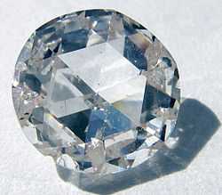
Chemical vapor deposition (CVD) can be used to produce a synthetic diamond by creating the circumstances necessary for carbon atoms in a gas to settle on a substrate in crystalline form.
CVD production of diamonds has received a great deal of attention in the materials sciences because it allows many new applications of diamonds that had previously been considered too difficult to make economical. CVD diamond growth typically occurs under low pressure (1–27 kPa; 0.145–3.926 psi; 7.5-203 Torr) and involves feeding varying amounts of gases into a chamber, energizing them and providing conditions for diamond growth on the substrate. The gases always include a carbon source, and typically include hydrogen as well, though the amounts used vary greatly depending on the type of diamond being grown. Energy sources include hot filament, microwave power, and arc discharges, among others. The energy source is intended to generate a plasma in which the gases are broken down and more complex chemistries occur. The actual chemical process for diamond growth is still under study and is complicated by the very wide variety of diamond growth processes used.
Using CVD, films of diamond can be grown over large areas of substrate with control over the properties of the diamond produced. In the past, when high pressure high temperature (HPHT) techniques were used to produce a diamond, the result was typically very small free standing diamonds of varying sizes. With CVD diamond growth areas of greater than fifteen centimeters (six inches) diameter have been achieved and much larger areas are likely to be successfully coated with diamond in the future. Improving this process is key to enabling several important applications.
The growth of diamond directly on a substrate allows the addition of many of diamond's important qualities to other materials. Since diamond has the highest thermal conductivity of any bulk material, layering diamond onto high heat producing electronics (such as optics and transistors) allows the diamond to be used as a heat sink.[14][15] Diamond films are being grown on valve rings, cutting tools, and other objects that benefit from diamond's hardness and exceedingly low wear rate. In each case the diamond growth must be carefully done to achieve the necessary adhesion onto the substrate. Diamond's very high scratch resistance and thermal conductivity, combined with a lower coefficient of thermal expansion than Pyrex glass, a coefficient of friction close to that of Teflon (Polytetrafluoroethylene) and strong lipophilicity would make it a nearly ideal non-stick coating for cookware if large substrate areas could be coated economically.
CVD growth allows one to control the properties of the diamond produced. In the area of diamond growth, the word "diamond" is used as a description of any material primarily made up of sp3 bonded carbon, and there are many different types of diamond included in this. By regulating the processing parameters—especially the gases introduced, but also including the pressure the system is operated under, the temperature of the diamond, and the method of generating plasma—many different materials that can be considered diamond can be made. Single crystal diamond can be made containing various dopants.[16] Polycrystalline diamond consisting of grain sizes from several nanometers to several micrometers can be grown.[14][17] Some polycrystalline diamond grains are surrounded by thin, non-diamond carbon, while others are not. These different factors affect the diamond's hardness, smoothness, conductivity, optical properties and more.
Chalcogenides
Commercially, mercury cadmium telluride is of continuing interest for detection of infrared radiation. Consisting of an alloy of CdTe and HgTe, this material can be prepared from the dimethyl derivatives of the respective elements.
See also
- Apollo Diamond
- Metalorganic Vapour Phase Epitaxy
- Atomic layer deposition
- Bubbler cylinder
- Carbonyl metallurgy
- Electrostatic spray assisted vapour deposition
- Element Six
- Ion plating
- Virtual metrology
References
- ↑ "Low Pressure Chemical Vapor Deposition – Technology and Equipment". Crystec Technology Trading GmbH.
- ↑ Crystec Technology Trading GmbH, Plasma Enhanced Chemical Vapor Deposition – Technology and Equipment
- ↑ Tavares, Jason; Swanson, E.J.; Coulombe, S. (2008). "Plasma Synthesis of Coated Metal Nanoparticles with Surface Properties Tailored for Dispersion". Plasma Processes and Polymers 5 (8): 759. doi:10.1002/ppap.200800074.
- ↑ Schropp, R.E.I.; B. Stannowski, A.M. Brockhoff, P.A.T.T. van Veenendaal and J.K. Rath. "Hot wire CVD of heterogeneous and polycrystalline silicon semiconducting thin films for application in thin film transistors and solar cells" (PDF). Materials Physics and Mechanics. pp. 73–82.
- ↑ Gleason, Karen K.; Kenneth K.S. Lau; Jeffrey A. Caulfield (2000). "Structure and Morphology of Fluorocarbon Films Grown by Hot Filament Chemical Vapor Deposition". Chemistry of Materials 12 (10): 3032. doi:10.1021/cm000499w.
- ↑ Dorval Dion, C.A.; Tavares, J.R. (2013). "Photo-Initiated Chemical Vapour Deposition as a Scalable Particle Functionalization Technology (A Practical Review)". Powder Technology. doi:10.1016/j.powtec.2013.02.024.
- ↑ Wahl, Georg et al. (2000) "Thin Films" in Ullmann's Encyclopedia of Industrial Chemistry, Wiley-VCH, Weinheim. doi:10.1002/14356007.a26_681
- ↑ Gleason, Karen; Ayse Asatekin; Miles C. Barr; Samaan H. Baxamusa; Kenneth K.S. Lau; Wyatt Tenhaeff; Jingjing Xu (May 2010). "Designing polymer surfaces via vapor deposition". Materials Today 13 (5): 26–33. doi:10.1016/S1369-7021(10)70081-X.
- ↑ Simmler, W. (2005), "Silicon Compounds, Inorganic", Ullmann's Encyclopedia of Industrial Chemistry, Weinheim: Wiley-VCH, doi:10.1002/14356007.a24_001
- ↑ Proceedings of the Third World Congress of Chemical Engineering, Tokyo, p. 290 (1986)
- ↑ Sze, S.M. (2008). Semiconductor devices: physics and technology. Wiley-India. p. 384. ISBN 81-265-1681-X.
- ↑ Maruyama, Toshiro (1994). "Electrochromic Properties of Niobium Oxide Thin Films Prepared by Chemical Vapor Deposition". Journal of the Electrochemical Society 141 (10): 2868. doi:10.1149/1.2059247.
- ↑ Rahtu, Antti (2002). Atomic Layer Deposition of High Permittivity Oxides: Film Growth and In Situ Studies (Thesis). University of Helsinki. ISBN 952-10-0646-3.
- ↑ 14.0 14.1 Costello, M; Tossell, D; Reece, D; Brierley, C; Savage, J (1994). "Diamond protective coatings for optical components". Diamond and Related Materials 3 (8): 1137–1141. Bibcode:1994DRM.....3.1137C. doi:10.1016/0925-9635(94)90108-2.
- ↑ Sun Lee, Woong; Yu, Jin (2005). "Comparative study of thermally conductive fillers in underfill for the electronic components". Diamond and Related Materials 14 (10): 1647–1653. Bibcode:2005DRM....14.1647S. doi:10.1016/j.diamond.2005.05.008.
- ↑ Isberg, J (2004). "Single crystal diamond for electronic applications". Diamond and Related Materials 13 (2): 320–324. Bibcode:2004DRM....13..320I. doi:10.1016/j.diamond.2003.10.017.
- ↑ Krauss, A (2001). "Ultrananocrystalline diamond thin films for MEMS and moving mechanical assembly devices". Diamond and Related Materials 10 (11): 1952–1961. Bibcode:2001DRM....10.1952K. doi:10.1016/S0925-9635(01)00385-5.
Further reading
- Jaeger, Richard C. (2002). "Film Deposition". Introduction to Microelectronic Fabrication (2nd ed.). Upper Saddle River: Prentice Hall. ISBN 0-201-44494-1.
- Smith, Donald (1995). Thin-Film Deposition: Principles and Practice. MacGraw-Hill. ISBN 0-07-058502-4.
- Dobkin and Zuraw (2003). Principles of Chemical Vapor Deposition. Kluwer. ISBN 1-4020-1248-9.
- K. Okada "Plasma-enhanced chemical vapor deposition of nanocrystalline diamond" Sci. Technol. Adv. Mater. 8 (2007) 624 free-download review
- T. Liu, D. Raabe and S. Zaefferer "A 3D tomographic EBSD analysis of a CVD diamond thin film" Sci. Technol. Adv. Mater. 9 (2008) 035013 free-download
- Christoph Wild "CVD Diamond Properties and Useful Formula" CVD Diamond Booklet (2008) PDF free-download
- Dennis W. Hess, CHEMICAL VAPOR DEPOSITION OF DIELECTRIC AND METAL FILMSfree-download from Electronic Materials and Processing: Proceedings of the First Electronic Materials and Processing Congress held in conjunction with the 1988 World Materials Congress Chicago, Illinois, USA, 24–30 September 1988, Edited by Prabjit Singh (Sponsored by the Electronic Materials and Processing Division of ASM INTERNATIONAL)
| ||||||||||||||||||||||||||||||