Channelling (physics)
Channelling is the process that constrains the path of a charged particle in a crystalline solid [1]
Many physical phenomena can occur when a charged particle is incident upon a solid target, e.g., elastic scattering, inelastic energy-loss processes, secondary-electron emission, electromagnetic radiation, nuclear reactions, etc. All of these processes have cross sections which depend on the impact parameters involved in collisions with individual target atoms. When the target material is homogeneous and isotropic, the impact-parameter distribution is independent of the orientation of the momentum of the particle and interaction processes are also orientation-independent. When the target material is monocrystalline, the yields of physical processes are very strongly dependent on the orientation of the momentum of the particle relative to the crystalline axes or planes. Or in other words, the stopping power of the particle is much lower in certain directions than others. This effect is commonly called the "channelling" effect. It is related to other orientation-dependent effects, such as particle diffraction. These relationships will be discussed in detail later.


History
The channelling effect was first discovered in binary collision approximation computer simulations in 1963 [1] to explain exponential tails in experimentally observed ion range distributions that did not conform to standard theories of ion penetration. The simulated prediction was confirmed experimentally the following year by measurements of ion penetration depths in single-crystalline tungsten.[2]
Mechanism
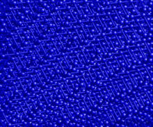
From a simple, classical standpoint, one may qualitatively understand the channelling effect as follows: If the direction of a charged particle incident upon the surface of a monocrystal lies close to a major crystal direction (Fig. 1), the particle with high probability will only do small-angle scattering as it passes through the several layers of atoms in the crystal and hence remain in the samel crystal 'channel'. If it is not in a major crystal direction or plane ("random direction", Fig. 2), it is much more likely to undergo large-angle scattering and hence its final mean penetration depth is likely to be shorter. If the direction of the particle's momentum is close to the crystalline plane, but it is not close to major crystalling axes, this phenomenon is called "plane channelling". Negatively charged particles like antiprotons and electrons are attracted towards the positively charged nuclei of the plane, and after passing the center of the plane, they will be attracted again, so negatively charged particles tend to follow the direction of one crystalline plane.


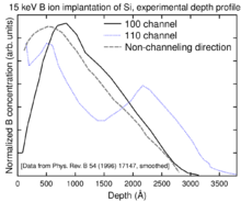
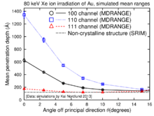
Channelling usually leads to deeper penetration of the ions in the material, an effect that has been observed experimentally and in computer simulations, see Figures 3 and 4.
Because the crystalline plane has a high density of atomic electrons and nuclei, the channeled particles eventually suffer a high angle Rutherford scattering or energy-losses in collision with electrons and leave the channel. This is called the "dechannelling" process.
Positively charged particles like protons and positrons are instead repelled from the nuclei of the plane, and after entering the space between two neighboring planes, they will be repelled from the second plane. So positively charged particles tend to follow the direction between two neighboring crystalline planes, but at the largest possible distance from each of them. Therefore, the positively charged particles have a smaller probability of interacting with the nuclei and electrons of the planes (smaller "dechannelling" effect) and travel longer distances.
The same phenomena occur when the direction of momentum of the charged particles lies close to a major crystalline, high-symmetry axis. This phenomenon is called "axial channelling".
At low energies the channelling effects in crystals are not present because small-angle scattering at low energies requires large impact parameters, which become bigger than interplanar distances. The particle's diffraction is dominating here. At high energies the quantum effects and diffraction are less effective and the channelling effect is present.
Applications
There are several particularly interesting applications of the channelling effects.
Channelling effects can be used as tools to investigate the properties of the crystal lattice and of its perturbations (like doping) in the bulk region that is not accessible to X-rays. This is an important variation of the Rutherford backscattering ion beam analysis technique, commonly called Rutherford backscattering/channeling (RBS-C).
At higher energies (tens of GeV), the applications include the channelling radiation for enhanced production of high energy gamma rays, and the use of bent crystals for extraction of particles from the halo of the circulating beam in an particle accelerator.
General literature
- J.W. Mayer and E. Rimini, Ion Beam Handbook for Material Analysis, (1977) Academic Press, New York
- L.C. Feldman, J.W. Mayer and S.T.Picraux, Material Analysis by Ion Channelling, (1982) Academic Press, New York
- R. Hovden, H. L. Xin, D. A. Muller, Phys. Rev. B 86, 195415 (2012)
- G. R. Anstis, D. Q. Cai, and D. J. H. Cockayne, Ultramicroscopy 94, 309 (2003).
- D. Van Dyck and J. H. Chen, Solid State Communications 109, 501 (1999).
- S. Hillyard and J. Silcox, Ultramicroscopy 58, 6 (1995).
- S. J. Pennycook and D. E. Jesson, Physical Review Letters 64, 938 (1990).
- M. V. Berry and Ozoriode.Am, Journal of Physics a-Mathematical and General 6, 1451 (1973).
- M. V. Berry, Journal of Physics Part C Solid State Physics 4, 697 (1971).
- A. Howie, Philosophical Magazine 14, 223 (1966).
- P. B. Hirsch, A. Howie, R. B. Nicholson, D. W. Pashley, and M. Whelan, Electron microscopy of thin crystals (Butterworths London, 1965).
References
- ↑ 1.0 1.1 M. T. Robinson and O. S. Oen, The channeling of energetic atoms in crystal lattices, Appl. Phys. Lett. 2 (1963) 30.
- ↑ E. V. Kornelsen, F. Brown, J. A. Davies, B. Domeij and G. R. Piercy, Penetration of Heavy Ions of keV Energies into Monocrystalline Tungsten, Phys. Rev. 136 (1964) 849
- ↑ David Cai, Niels Gronbech-Jensen, Charles M. Snell, and Keith M. Beardmore. Phenomenological electronic stopping-power model for molecular dynamics and monte carlo simulation of ion implantation into silicon. Phys. Rev. B, 54(23):17147, 1996.
- ↑ K. Nordlund. Molecular dynamics simulation of ion ranges in the 1 -- 100 kev energy range. Comput. Mater. Sci., 3:448, 1995
- ↑ G. Greaves, J. A. Hinks, P. Busby, N. J. Mellors, A. Ilinov, A. Kuronen, K. Nordlund, and S. E. Donnelly. Giant sputtering yields from single-ion impacts on gold nanorods. Phys. Rev. Lett., 111:065504, 2013
- ↑ J. L. Whitton, Canadian Journal of Physics, 1967, 45(5): 1947-1957.
External links
- nice animation
- CERN NA43 Experiment that investigated interactions of high energy particles with crystals
- Note and reports on crystal extraction
- The future looks bright for particle channelling on CERN Courier