Bipolar junction transistor
.svg.png) | PNP |
.svg.png) | NPN |
PNP- and NPN-type
BJTs.
A bipolar junction transistor (BJT or bipolar transistor) is a type of transistor that relies on the contact of two types of semiconductor for its operation. BJTs can be used as amplifiers, switches, or in oscillators. BJTs can be found either as individual discrete components, or in large numbers as parts of integrated circuits.
Bipolar transistors are so named because their operation involves both electrons and holes. These two kinds of charge carriers are characteristic of the two kinds of doped semiconductor material; electrons are majority charge carriers in n-type semiconductors, whereas holes are majority charge carriers in p-type semiconductors. In contrast, unipolar transistors such as the field-effect transistors have only one kind of charge carrier.
Charge flow in a BJT is due to diffusion of charge carriers across a junction between two regions of different charge concentrations. The regions of a BJT are called emitter, collector, and base.[note 1] A discrete transistor has three leads for connection to these regions. Typically, the emitter region is heavily doped compared to the other two layers, whereas the majority charge carrier concentrations in base and collector layers are about the same. By design, most of the BJT collector current is due to the flow of charges injected from a high-concentration emitter into the base where there are minority carriers that diffuse toward the collector, and so BJTs are classified as minority-carrier devices.
Introduction
.svg.png)
BJTs come in two types, or polarities, known as PNP and NPN based on the doping types of the three main terminal regions. An NPN transistor comprises two semiconductor junctions that share a thin p-doped anode region, and a PNP transistor comprises two semiconductor junctions that share a thin n-doped cathode region.
In typical operation, the base–emitter junction is forward biased, which means that the p-doped side of the junction is at a more positive potential than the n-doped side, and the base–collector junction is reverse biased. In an NPN transistor, when positive bias is applied to the base–emitter junction, the equilibrium is disturbed between the thermally generated carriers and the repelling electric field of the n-doped emitter depletion region. This allows thermally excited electrons to inject from the emitter into the base region. These electrons diffuse through the base from the region of high concentration near the emitter towards the region of low concentration near the collector. The electrons in the base are called minority carriers because the base is doped p-type, which makes holes the majority carrier in the base.
To minimize the percentage of carriers that recombine before reaching the collector–base junction, the transistor's base region must be thin enough that carriers can diffuse across it in much less time than the semiconductor's minority carrier lifetime. In particular, the thickness of the base must be much less than the diffusion length of the electrons. The collector–base junction is reverse-biased, and so little electron injection occurs from the collector to the base, but electrons that diffuse through the base towards the collector are swept into the collector by the electric field in the depletion region of the collector–base junction. The thin shared base and asymmetric collector–emitter doping is what differentiates a bipolar transistor from two separate and oppositely biased diodes connected in series.
Voltage, current, and charge control
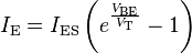
The collector–emitter current can be viewed as being controlled by the base–emitter current (current control), or by the base–emitter voltage (voltage control). These views are related by the current–voltage relation of the base–emitter junction, which is just the usual exponential current–voltage curve of a p-n junction (diode).[1]
The physical explanation for collector current is the amount of minority carriers in the base region.[1][2][3] Due to low level injection (in which there are much fewer excess carriers than normal majority carriers) the ambipolar transport rates (in which the excess majority and minority carriers flow at the same rate) is in effect determined by the excess minority carriers.
Detailed transistor models of transistor action, such as the Gummel–Poon model, account for the distribution of this charge explicitly to explain transistor behaviour more exactly.[4] The charge-control view easily handles phototransistors, where minority carriers in the base region are created by the absorption of photons, and handles the dynamics of turn-off, or recovery time, which depends on charge in the base region recombining. However, because base charge is not a signal that is visible at the terminals, the current- and voltage-control views are generally used in circuit design and analysis.
In analog circuit design, the current-control view is sometimes used because it is approximately linear. That is, the collector current is approximately  times the base current. Some basic circuits can be designed by assuming that the emitter–base voltage is approximately constant, and that collector current is beta times the base current. However, to accurately and reliably design production BJT circuits, the voltage-control (for example, Ebers–Moll) model is required.[1] The voltage-control model requires an exponential function to be taken into account, but when it is linearized such that the transistor can be modelled as a transconductance, as in the Ebers–Moll model, design for circuits such as differential amplifiers again becomes a mostly linear problem, so the voltage-control view is often preferred. For translinear circuits, in which the exponential I–V curve is key to the operation, the transistors are usually modelled as voltage controlled with transconductance proportional to collector current. In general, transistor level circuit design is performed using SPICE or a comparable analog circuit simulator, so model complexity is usually not of much concern to the designer.
Turn-on, turn-off, and storage delay
The Bipolar transistor exhibits a few delay characteristics when turning on and off. Most transistors, and especially power transistors, exhibit long base-storage times that limit maximum frequency of operation in switching applications. One method for reducing this storage time is by using a Baker clamp.
Transistor parameters: alpha (α) and beta (β)
The proportion of electrons able to cross the base and reach the collector is a measure of the BJT efficiency. The heavy doping of the emitter region and light doping of the base region causes many more electrons to be injected from the emitter into the base than holes to be injected from the base into the emitter.
The common-emitter current gain is represented by βF or the h-parameter hFE; it is approximately the ratio of the DC collector current to the DC base current in forward-active region. It is typically greater than 50 for small-signal transistors but can be smaller in transistors designed for high-power applications.
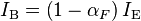
Another important parameter is the common-base current gain, αF. The common-base current gain is approximately the gain of current from emitter to collector in the forward-active region. This ratio usually has a value close to unity; between 0.98 and 0.998. It is less than unity due to recombination of charge carriers as they cross the base region. Alpha and beta are more precisely related by the following identities (NPN transistor):


Structure
_Cross-section.svg)
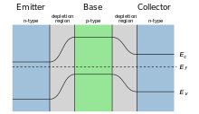
A BJT consists of three differently doped semiconductor regions, the emitter region, the base region and the collector region. These regions are, respectively, p type, n type and p type in a PNP transistor, and n type, p type and n type in an NPN transistor. Each semiconductor region is connected to a terminal, appropriately labeled: emitter (E), base (B) and collector (C).
The base is physically located between the emitter and the collector and is made from lightly doped, high resistivity material. The collector surrounds the emitter region, making it almost impossible for the electrons injected into the base region to escape without being collected, thus making the resulting value of α very close to unity, and so, giving the transistor a large β. A cross section view of a BJT indicates that the collector–base junction has a much larger area than the emitter–base junction.
The bipolar junction transistor, unlike other transistors, is usually not a symmetrical device. This means that interchanging the collector and the emitter makes the transistor leave the forward active mode and start to operate in reverse mode. Because the transistor's internal structure is usually optimized for forward-mode operation, interchanging the collector and the emitter makes the values of α and β in reverse operation much smaller than those in forward operation; often the α of the reverse mode is lower than 0.5. The lack of symmetry is primarily due to the doping ratios of the emitter and the collector. The emitter is heavily doped, while the collector is lightly doped, allowing a large reverse bias voltage to be applied before the collector–base junction breaks down. The collector–base junction is reverse biased in normal operation. The reason the emitter is heavily doped is to increase the emitter injection efficiency: the ratio of carriers injected by the emitter to those injected by the base. For high current gain, most of the carriers injected into the emitter–base junction must come from the emitter.
The low-performance "lateral" bipolar transistors sometimes used in CMOS processes are sometimes designed symmetrically, that is, with no difference between forward and backward operation.
Small changes in the voltage applied across the base–emitter terminals causes the current that flows between the emitter and the collector to change significantly. This effect can be used to amplify the input voltage or current. BJTs can be thought of as voltage-controlled current sources, but are more simply characterized as current-controlled current sources, or current amplifiers, due to the low impedance at the base.
Early transistors were made from germanium but most modern BJTs are made from silicon. A significant minority are also now made from gallium arsenide, especially for very high speed applications (see HBT, below).
NPN
NPN is one of the two types of bipolar transistors, consisting of a layer of P-doped semiconductor (the "base") between two N-doped layers. A small current entering the base is amplified to produce a large collector and emitter current. That is, when there is a positive potential difference measured from the emitter of an NPN transistor to its base (i.e., when the base is high relative to the emitter) as well as positive potential difference measured from the base to the collector, the transistor becomes active. In this "on" state, current flows between the collector and emitter of the transistor. Most of the current is carried by electrons moving from emitter to collector as minority carriers in the P-type base region. To allow for greater current and faster operation, most bipolar transistors used today are NPN because electron mobility is higher than hole mobility.
A mnemonic device for the NPN transistor symbol is "not pointing in", based on the arrows in the symbol and the letters in the name.[5]
PNP
The other type of BJT is the PNP, consisting of a layer of N-doped semiconductor between two layers of P-doped material. A small current leaving the base is amplified in the collector output. That is, a PNP transistor is "on" when its base is pulled low relative to the emitter.
The arrows in the NPN and PNP transistor symbols are on the emitter legs and point in the direction of the conventional current flow when the device is in forward active mode.
A mnemonic device for the PNP transistor symbol is "pointing in (proudly/permanently)", based on the arrows in the symbol and the letters in the name.[6]
Heterojunction bipolar transistor
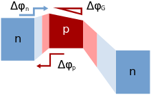
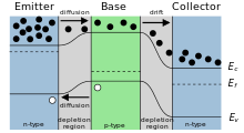
The heterojunction bipolar transistor (HBT) is an improvement of the BJT that can handle signals of very high frequencies up to several hundred GHz. It is common in modern ultrafast circuits, mostly RF systems.[7][8] Heterojunction transistors have different semiconductors for the elements of the transistor. Usually the emitter is composed of a larger bandgap material than the base. The figure shows that this difference in bandgap allows the barrier for holes to inject backward from the base into the emitter, denoted in the figure as Δφp, to be made large, while the barrier for electrons to inject into the base Δφn is made low. This barrier arrangement helps reduce minority carrier injection from the base when the emitter-base junction is under forward bias, and thus reduces base current and increases emitter injection efficiency.
The improved injection of carriers into the base allows the base to have a higher doping level, resulting in lower resistance to access the base electrode. In the more traditional BJT, also referred to as homojunction BJT, the efficiency of carrier injection from the emitter to the base is primarily determined by the doping ratio between the emitter and base, which means the base must be lightly doped to obtain high injection efficiency, making its resistance relatively high. In addition, higher doping in the base can improve figures of merit like the Early voltage by lessening base narrowing.
The grading of composition in the base, for example, by progressively increasing the amount of germanium in a SiGe transistor, causes a gradient in bandgap in the neutral base, denoted in the figure by ΔφG, providing a "built-in" field that assists electron transport across the base. That drift component of transport aids the normal diffusive transport, increasing the frequency response of the transistor by shortening the transit time across the base.
Two commonly used HBTs are silicon–germanium and aluminum gallium arsenide, though a wide variety of semiconductors may be used for the HBT structure. HBT structures are usually grown by epitaxy techniques like MOCVD and MBE.
Regions of operation
| Applied voltages | B-E junction bias (NPN) | B-C junction bias (NPN) | Mode (NPN) |
|---|---|---|---|
| E < B < C | Forward | Reverse | Forward-active |
| E < B > C | Forward | Forward | Saturation |
| E > B < C | Reverse | Reverse | Cut-off |
| E > B > C | Reverse | Forward | Reverse-active |
| Applied voltages | B-E junction bias (PNP) | B-C junction bias (PNP) | Mode (PNP) |
| E < B < C | Reverse | Forward | Reverse-active |
| E < B > C | Reverse | Reverse | Cut-off |
| E > B < C | Forward | Forward | Saturation |
| E > B > C | Forward | Reverse | Forward-active |
 ,
,  and
and  .
.Bipolar transistors have five distinct regions of operation, defined by BJT junction biases.
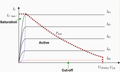
- Forward-active (or simply, active): The base–emitter junction is forward biased and the base–collector junction is reverse biased. Most bipolar transistors are designed to afford the greatest common-emitter current gain, βF, in forward-active mode. If this is the case, the collector–emitter current is approximately proportional to the base current, but many times larger, for small base current variations.
- Reverse-active (or inverse-active or inverted): By reversing the biasing conditions of the forward-active region, a bipolar transistor goes into reverse-active mode. In this mode, the emitter and collector regions switch roles. Because most BJTs are designed to maximize current gain in forward-active mode, the βF in inverted mode is several times smaller (2–3 times for the ordinary germanium transistor). This transistor mode is seldom used, usually being considered only for failsafe conditions and some types of bipolar logic. The reverse bias breakdown voltage to the base may be an order of magnitude lower in this region.
- Saturation: With both junctions forward-biased, a BJT is in saturation mode and facilitates high current conduction from the emitter to the collector (or the other direction in the case of NPN, with negatively charged carriers flowing from emitter to collector). This mode corresponds to a logical "on", or a closed switch.
- Cutoff: In cutoff, biasing conditions opposite of saturation (both junctions reverse biased) are present. There is very little current, which corresponds to a logical "off", or an open switch.
- Avalanche breakdown region
The modes of operation can be described in terms of the applied voltages (this description applies to NPN transistors; polarities are reversed for PNP transistors):
- Forward-active: base higher than emitter, collector higher than base (in this mode the collector current is proportional to base current by ).
- Saturation: base higher than emitter, but collector is not higher than base.
- Cut-Off: base lower than emitter, but collector is higher than base. It means the transistor is not letting conventional current go through from collector to emitter.
- Reverse-active: base lower than emitter, collector lower than base: reverse conventional current goes through transistor.
In terms of junction biasing: ('reverse biased base–collector junction' means Vbc < 0 for NPN, opposite for PNP)
Although these regions are well defined for sufficiently large applied voltage, they overlap somewhat for small (less than a few hundred millivolts) biases. For example, in the typical grounded-emitter configuration of an NPN BJT used as a pulldown switch in digital logic, the "off" state never involves a reverse-biased junction because the base voltage never goes below ground; nevertheless the forward bias is close enough to zero that essentially no current flows, so this end of the forward active region can be regarded as the cutoff region.
Active-mode NPN transistors in circuits

The diagram shows a schematic representation of an NPN transistor connected to two voltage sources. To make the transistor conduct appreciable current (on the order of 1 mA) from C to E, VBE must be above a minimum value sometimes referred to as the cut-in voltage. The cut-in voltage is usually about 650 mV for silicon BJTs at room temperature but can be different depending on the type of transistor and its biasing. This applied voltage causes the lower P-N junction to 'turn on', allowing a flow of electrons from the emitter into the base. In active mode, the electric field existing between base and collector (caused by VCE) will cause the majority of these electrons to cross the upper P-N junction into the collector to form the collector current IC. The remainder of the electrons recombine with holes, the majority carriers in the base, making a current through the base connection to form the base current, IB. As shown in the diagram, the emitter current, IE, is the total transistor current, which is the sum of the other terminal currents, (i.e., IE = IB + IC).
In the diagram, the arrows representing current point in the direction of conventional current – the flow of electrons is in the opposite direction of the arrows because electrons carry negative electric charge. In active mode, the ratio of the collector current to the base current is called the DC current gain. This gain is usually 100 or more, but robust circuit designs do not depend on the exact value (for example see op-amp). The value of this gain for DC signals is referred to as  , and the value of this gain for small signals is referred to as
  . That is, when a small change in the currents occurs, and sufficient time has passed for the new condition to reach a steady state is the ratio of the change in collector current to the change in base current. The symbol
  is used for both and .[9]
The emitter current is related to  exponentially. At room temperature, an increase in by approximately 60 mV increases the emitter current by a factor of 10. Because the base current is approximately proportional to the collector and emitter currents, they vary in the same way.
Active-mode PNP transistors in circuits

The diagram shows a schematic representation of a PNP transistor connected to two voltage sources. To make the transistor conduct appreciable current (on the order of 1 mA) from E to C,  must be above a minimum value sometimes referred to as the cut-in voltage. The cut-in voltage is usually about 650 mV for silicon BJTs at room temperature but can be different depending on the type of transistor and its biasing. This applied voltage causes the upper P-N junction to 'turn-on' allowing a flow of holes from the emitter into the base. In active mode, the electric field existing between the emitter and the collector (caused by
  ) causes the majority of these holes to cross the lower p-n junction into the collector to form the collector current
  . The remainder of the holes recombine with electrons, the majority carriers in the base, making a current through the base connection to form the base current,
  . As shown in the diagram, the emitter current,
  , is the total transistor current, which is the sum of the other terminal currents (i.e., IE = IB + IC).
In the diagram, the arrows representing current point in the direction of conventional current – the flow of holes is in the same direction of the arrows because holes carry positive electric charge. In active mode, the ratio of the collector current to the base current is called the DC current gain. This gain is usually 100 or more, but robust circuit designs do not depend on the exact value. The value of this gain for DC signals is referred to as , and the value of this gain for AC signals is referred to as . However, when there is no particular frequency range of interest, the symbol is used.
It should also be noted that the emitter current is related to exponentially. At room temperature, an increase in by approximately 60 mV increases the emitter current by a factor of 10. Because the base current is approximately proportional to the collector and emitter currents, they vary in the same way.
History
The bipolar point-contact transistor was invented in December 1947 at the Bell Telephone Laboratories by John Bardeen and Walter Brattain under the direction of William Shockley. The junction version known as the bipolar junction transistor, invented by Shockley in 1948, enjoyed three decades as the device of choice in the design of discrete and integrated circuits. Nowadays, the use of the BJT has declined in favor of CMOS technology in the design of digital integrated circuits. The incidental low performance BJTs inherent in CMOS ICs, however, are often utilized as bandgap voltage reference, silicon bandgap temperature sensor and to handle electrostatic discharge.
Germanium transistors
The germanium transistor was more common in the 1950s and 1960s, and while it exhibits a lower "cut off" voltage, typically around 0.2 V, making it more suitable for some applications, it also has a greater tendency to exhibit thermal runaway.
Early manufacturing techniques
Various methods of manufacturing bipolar transistors were developed.[10]
Bipolar transistors
- Point-contact transistor – first transistor ever constructed (December 1947), a bipolar transistor, limited commercial use due to high cost and noise.
- Tetrode point-contact transistor – Point-contact transistor having two emitters. It became obsolete in the middle 1950s.
- Junction transistors
- Grown-junction transistor – first bipolar junction transistor made.[11] Invented by William Shockley at Bell Labs. Invented on June 23, 1948.[12] Patent filed on June 26, 1948.
- Alloy-junction transistor – emitter and collector alloy beads fused to base. Developed at General Electric and RCA[13] in 1951.
- Micro-alloy transistor (MAT) – high speed type of alloy junction transistor. Developed at Philco.[14]
- Micro-alloy diffused transistor (MADT) – high speed type of alloy junction transistor, speedier than MAT, a diffused-base transistor. Developed at Philco.
- Post-alloy diffused transistor (PADT) – high speed type of alloy junction transistor, speedier than MAT, a diffused-base transistor. Developed at Philips.
- Tetrode transistor – high speed variant of grown-junction transistor[15] or alloy junction transistor[16] with two connections to base.
- Surface-barrier transistor – high speed metal barrier junction transistor. Developed at Philco[17] in 1953.[18]
- Drift-field transistor – high speed bipolar junction transistor. Invented by Herbert Kroemer[19][20] at the Central Bureau of Telecommunications Technology of the German Postal Service, in 1953.
- Spacistor – circa 1957.
- Diffusion transistor – modern type bipolar junction transistor. Prototypes[21] developed at Bell Labs in 1954.
- Diffused-base transistor – first implementation of diffusion transistor.
- Mesa transistor – Developed at Texas Instruments in 1957.
- Planar transistor – the bipolar junction transistor that made mass-produced monolithic integrated circuits possible. Developed by Dr. Jean Hoerni[22] at Fairchild in 1959.
- Epitaxial transistor – a bipolar junction transistor made using vapor phase deposition. See epitaxy. Allows very precise control of doping levels and gradients.
Theory and modeling
Transistors can be thought of as two diodes (P–N junctions) sharing a common region that minority carriers can move through. A PNP BJT will function like two diodes that share an N-type cathode region, and the NPN like two diodes sharing a P-type anode region. Connecting two diodes with wires will not make a transistor, since minority carriers will not be able to get from one P–N junction to the other through the wire.
Both types of BJT function by letting a small current input to the base control an amplified output from the collector. The result is that the transistor makes a good switch that is controlled by its base input. The BJT also makes a good amplifier, since it can multiply a weak input signal to about 100 times its original strength. Networks of transistors are used to make powerful amplifiers with many different applications. In the discussion below, focus is on the NPN bipolar transistor. In the NPN transistor in what is called active mode, the base–emitter voltage and collector–base voltage  are positive, forward biasing the emitter–base junction and reverse-biasing the collector–base junction. In the active mode of operation, electrons are injected from the forward biased n-type emitter region into the p-type base where they diffuse as minority carriers to the reverse-biased n-type collector and are swept away by the electric field in the reverse-biased collector–base junction. For a figure describing forward and reverse bias, see semiconductor diodes.
Large-signal models
In 1954 Jewell James Ebers and John L. Moll introduced their mathematical model of transistor currents:[23]
Ebers–Moll model
.svg)
.svg)

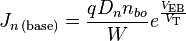
The DC emitter and collector currents in active mode are well modeled by an approximation to the Ebers–Moll model:

The base internal current is mainly by diffusion (see Fick's law) and
where
-
 is the thermal voltage
  (approximately 26 mV at 300 K ≈ room temperature).
 - is the emitter current
- is the collector current
-
 is the common base forward short circuit current gain (0.98 to 0.998)
 -
 is the reverse saturation current of the base–emitter diode (on the order of 10−15 to 10−12 amperes)
 - is the base–emitter voltage
-
 is the diffusion constant for electrons in the p-type base
 - W is the base width
The  and forward parameters are as described previously. A reverse is sometimes included in the model.
The unapproximated Ebers–Moll equations used to describe the three currents in any operating region are given below. These equations are based on the transport model for a bipolar junction transistor.[25]
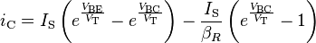
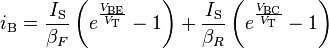
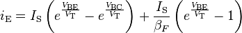
where
-
 is the collector current
 -
 is the base current
 -
 is the emitter current
 - is the forward common emitter current gain (20 to 500)
-
 is the reverse common emitter current gain (0 to 20)
 -
 is the reverse saturation current (on the order of 10−15 to 10−12 amperes)
 - is the thermal voltage (approximately 26 mV at 300 K ≈ room temperature).
- is the base–emitter voltage
-
 is the base–collector voltage
Base-width modulation
.svg)
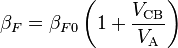
As the collector–base voltage ( ) varies, the collector–base depletion region varies in size. An increase in the collector–base voltage, for example, causes a greater reverse bias across the collector–base junction, increasing the collector–base depletion region width, and decreasing the width of the base. This variation in base width often is called the "Early effect" after its discoverer James M. Early.
Narrowing of the base width has two consequences:
- There is a lesser chance for recombination within the "smaller" base region.
- The charge gradient is increased across the base, and consequently, the current of minority carriers injected across the emitter junction increases.
Both factors increase the collector or "output" current of the transistor in response to an increase in the collector–base voltage.
In the forward-active region, the Early effect modifies the collector current () and the forward common emitter current gain () as given by:
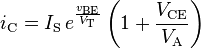

where:
- is the collector–emitter voltage
-
 is the Early voltage (15 V to 150 V)
 -
 is forward common-emitter current gain when = 0 V
 -
 is the output impedance
 - is the collector current
Punchthrough
When the base–collector voltage reaches a certain (device specific) value, the base–collector depletion region boundary meets the base–emitter depletion region boundary. When in this state the transistor effectively has no base. The device thus loses all gain when in this state.
Gummel–Poon charge-control model
The Gummel–Poon model[26] is a detailed charge-controlled model of BJT dynamics, which has been adopted and elaborated by others to explain transistor dynamics in greater detail than the terminal-based models typically do . This model also includes the dependence of transistor -values upon the direct current levels in the transistor, which are assumed current-independent in the Ebers–Moll model.[27]
Small-signal models
hybrid-pi model
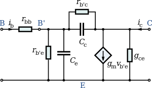
The hybrid-pi model is a popular circuit model used for analyzing the small signal behavior of bipolar junction and field effect transistors. Sometimes it is also called Giacoletto model because it was introduced by L.J. Giacoletto in 1969. The model can be quite accurate for low-frequency circuits and can easily be adapted for higher frequency circuits with the addition of appropriate inter-electrode capacitances and other parasitic elements.
h-parameter model
.svg)
Another model commonly used to analyze BJT circuits is the "h-parameter" model, closely related to the hybrid-pi model and the y-parameter two-port, but using input current and output voltage as independent variables, rather than input and output voltages. This two-port network is particularly suited to BJTs as it lends itself easily to the analysis of circuit behaviour, and may be used to develop further accurate models. As shown, the term "x" in the model represents a different BJT lead depending on the topology used. For common-emitter mode the various symbols take on the specific values as:
- x = 'e' because it is a common-emitter topology
- Terminal 1 = Base
- Terminal 2 = Collector
- Terminal 3 = Emitter
- ii = Base current (ib)
- io = Collector current (ic)
- Vin = Base-to-emitter voltage (VBE)
- Vo = Collector-to-emitter voltage (VCE)
and the h-parameters are given by:
- hix = hie – The input impedance of the transistor (corresponding to the base resistance rpi).
- hrx = hre – Represents the dependence of the transistor's IB–VBE curve on the value of VCE. It is usually very small and is often neglected (assumed to be zero).
- hfx = hfe – The current-gain of the transistor. This parameter is often specified as hFE or the DC current-gain (βDC) in datasheets.
- hox = 1/hoe – The output impedance of transistor. The parameter hoe usually corresponds to the output admittance of the bipolar transistor and has to be inverted to convert it to an impedance.
As shown, the h-parameters have lower-case subscripts and hence signify AC conditions or analyses. For DC conditions they are specified in upper-case. For the CE topology, an approximate h-parameter model is commonly used which further simplifies the circuit analysis. For this the hoe and hre parameters are neglected (that is, they are set to infinity and zero, respectively). It should also be noted that the h-parameter model as shown is suited to low-frequency, small-signal analysis. For high-frequency analyses the inter-electrode capacitances that are important at high frequencies must be added.
Etymology of hFE
The 'h' refers to its being an h-parameter, a set of parameters named for their origin in a hybrid equivalent circuit model. 'F' is from forward current amplification also called the current gain. 'E' refers to the transistor operating in a common emitter (CE) configuration. Capital letters used in the subscript indicate that hFE refers to a direct current circuit.
Industry models
The Gummel Poon SPICE model is often used, but it suffers from several limitations. These have been addressed in various more advanced models: Mextram, VBIC, HICUM, Modella.[28][29][30][31]
Applications
The BJT remains a device that excels in some applications, such as discrete circuit design, due to the very wide selection of BJT types available, and because of its high transconductance and output resistance compared to MOSFETs. The BJT is also the choice for demanding analog circuits, especially for very-high-frequency applications, such as radio-frequency circuits for wireless systems. Bipolar transistors can be combined with MOSFETs in an integrated circuit by using a BiCMOS process of wafer fabrication to create circuits that take advantage of the application strengths of both types of transistor.
Amplifiers
The transistor parameters α and β characterizes the current gain of the BJT. It is this gain that allow BJTs to be used as the building blocks of electronic amplifiers. The three main BJT amplifier topologies are
Temperature sensors
Because of the known temperature and current dependence of the forward-biased base–emitter junction voltage, the BJT can be used to measure temperature by subtracting two voltages at two different bias currents in a known ratio .
Logarithmic converters
Because base–emitter voltage varies as the log of the base–emitter and collector–emitter currents, a BJT can also be used to compute logarithms and anti-logarithms. A diode can also perform these nonlinear functions but the transistor provides more circuit flexibility.
Vulnerabilities
Exposure of the transistor to ionizing radiation causes radiation damage. Radiation causes a buildup of 'defects' in the base region that act as recombination centers. The resulting reduction in minority carrier lifetime causes gradual loss of gain of the transistor.
Power BJTs are subject to a failure mode called secondary breakdown, in which excessive current and normal imperfections in the silicon die cause portions of the silicon inside the device to become disproportionately hotter than the others. The doped silicon has a negative temperature coefficient, meaning that it conducts more current at higher temperatures. Thus, the hottest part of the die conducts the most current, causing its conductivity to increase, which then causes it to become progressively hotter again, until the device fails internally. The thermal runaway process associated with secondary breakdown, once triggered, occurs almost instantly and may catastrophically damage the transistor package.
If the emitter-base junction is reverse biased into avalanche or Zener mode and current flows for a short period of time, the current gain of the BJT will be permanently degraded.
See also
Notes
- ↑ See point-contact transistor for the historical origin of these names.
References
- ↑ 1.0 1.1 1.2 Paul Horowitz and Winfield Hill (1989). The Art of Electronics (2nd ed.). Cambridge University Press. ISBN 978-0-521-37095-0.
- ↑ Juin Jei Liou and Jiann S. Yuan (1998). Semiconductor Device Physics and Simulation. Springer. ISBN 0-306-45724-5.
- ↑ General Electric (1962). Transistor Manual (6th ed.). p. 12. "If the principle of space charge neutrality is used in the analysis of the transistor, it is evident that the collector current is controlled by means of the positive charge (hole concentration) in the base region. ... When a transistor is used at higher frequencies, the fundamental limitation is the time it takes the carriers to diffuse across the base region..." (same in 4th and 5th editions)
- ↑ Paolo Antognetti and Giuseppe Massobrio (1993). Semiconductor Device Modeling with Spice. McGraw–Hill Professional. ISBN 0-07-134955-3.
- ↑ Alphonse J. Sistino (1996). Essentials of electronic circuitry. CRC Press. p. 64. ISBN 978-0-8247-9693-8.
- ↑ Alphonse J. Sistino (1996). Essentials of electronic circuitry. CRC Press. p. 102. ISBN 978-0-8247-9693-8.
- ↑ D.V. Morgan, Robin H. Williams (Editors) (1991). Physics and Technology of Heterojunction Devices. London: Institution of Electrical Engineers (Peter Peregrinus Ltd.). ISBN 0-86341-204-1.
- ↑ Peter Ashburn (2003). SiGe Heterojunction Bipolar Transistors. New York: Wiley. Chapter 10. ISBN 0-470-84838-3.
- ↑ Paul Horowitz and Winfield Hill (1989). The Art of Electronics (2nd ed.). Cambridge University Press. pp. 62–66. ISBN 978-0-521-37095-0.
- ↑ Third case study – the solid state advent (PDF)
- ↑ Transistor Museum, Historic Transistor Photo Gallery, Bell Labs Type M1752
- ↑ Morris, Peter Robin (1990). "4.2". A History of the World Semiconductor Industry. IEE History of Technology Series 12. London: Peter Peregrinus Ltd. p. 29. ISBN 0-86341-227-0.
- ↑ Transistor Museum, Historic Transistor Photo Gallery, RCA TA153
- ↑ High Speed Switching Transistor Handbook (2nd ed.). Motorola. 1963. p. 17.
- ↑ Transistor Museum, Historic Transistor Photo Gallery, Western Electric 3N22
- ↑ The Tetrode Power Transistor PDF
- ↑ Transistor Museum, Historic Transistor Photo Gallery, Philco A01
- ↑ Transistor Museum, Historic Transistor Photo Gallery, Surface Barrier Transistor
- ↑ Herb’s Bipolar Transistors IEEE Transactions on Electron Devices, vol. 48, no. 11, November 2001 PDF
- ↑ Influence of Mobility and Lifetime Variations on Drift-Field Effects in Silicon-Junction Devices PDF
- ↑ Transistor Museum, Historic Transistor Photo Gallery, Bell Labs Prototype Diffused Base Triode
- ↑ Transistor Museum, Historic Transistor Photo Gallery, Fairchild 2N1613
- ↑ J.J. Ebers and J.L Moll (1954) "Large-signal behavior of junction transistors", Proceedings of the Institute of Radio Engineers, 42 (12) : 1761–1772.
- ↑ Adel S. Sedra and Kenneth C. Smith (1987). Microelectronic Circuits, second ed. p. 903. ISBN 0-03-007328-6.
- ↑ A.S. Sedra and K.C. Smith (2004). Microelectronic Circuits (5th ed.). New York: Oxford. Eqs. 4.103–4.110, p. 305. ISBN 0-19-514251-9.
- ↑ H. K. Gummel and R. C. Poon, "An integral charge control model of bipolar transistors," Bell Syst. Tech. J., vol. 49, pp. 827–852, May–June 1970
- ↑ A.S. Sedra and K.C. Smith (2004). Microelectronic Circuits (5th ed.). New York: Oxford. p. 509. ISBN 0-19-514251-9.
- ↑ http://www.silvaco.com/content/kbase/smartspice_device_models.pdf
- ↑ Gennady Gildenblat, ed. (2010). Compact Modeling: Principles, Techniques and Applications. Springer Science & Business Media. Part II Compact Models of Bipolar Junction Transistors, pp. 167-267 cover Mextram and HiCuM in-depth. ISBN 978-90-481-8614-3.
- ↑ Michael Schröter (2010). Compact Hierarchical Bipolar Transistor Modeling with Hicum. World Scientific. ISBN 978-981-4273-21-3.
- ↑ http://joerg-berkner.de/Fachartikel/pdf/2002_ICCAP_UM_Berkner_Compact_Models_4_BJTs.pdf
External links
| Wikimedia Commons has media related to Bipolar junction transistors. |
- Simulation of a BJT in the Common Emitter Circuit
- Lessons In Electric Circuits – Bipolar Junction Transistors (Note: this site shows current as a flow of electrons, rather than the convention of showing it as a flow of holes)
- EncycloBEAMia – Bipolar Junction Transistor
- Characteristic curves
- ENGI 242/ELEC 222: BJT Small Signal Models
- Transistor Museum, Historic Transistor Timeline
- ECE 327: Transistor Basics – Summarizes simple Ebers–Moll model of a bipolar transistor and gives several common BJT circuits.
- ECE 327: Procedures for Output Filtering Lab – Section 4 ("Power Amplifier") discusses design of a BJT-Sziklai-pair-based class-AB current driver in detail.
- BJT Operation description for undergraduate and first year graduate students to describe the basic principles of operation of Bipolar Junction Transistor.
| ||||||||||||||||||
| ||||||||||||||||||||||||||||||||||
|