Band gap
In solid-state physics, a band gap, also called an energy gap or bandgap, is an energy range in a solid where no electron states can exist. In graphs of the electronic band structure of solids, the band gap generally refers to the energy difference (in electron volts) between the top of the valence band and the bottom of the conduction band in insulators and semiconductors. This is equivalent to the energy required to free an outer shell electron from its orbit about the nucleus to become a mobile charge carrier, able to move freely within the solid material, so the band gap is a major factor determining the electrical conductivity of a solid. Substances with large band gaps are generally insulators, those with smaller band gaps are semiconductors, while conductors either have very small band gaps or none, because the valence and conduction bands overlap.
In semiconductor physics
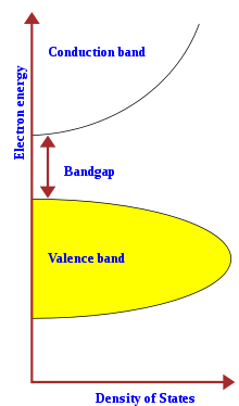
Every solid has its own characteristic energy-band structure. This variation in band structure is responsible for the wide range of electrical characteristics observed in various materials. In semiconductors and insulators, electrons are confined to a number of bands of energy, and forbidden from other regions. The term "band gap" refers to the energy difference between the top of the valence band and the bottom of the conduction band. Electrons are able to jump from one band to another. However, in order for an electron to jump from a valence band to a conduction band, it requires a specific minimum amount of energy for the transition. The required energy differs with different materials. Electrons can gain enough energy to jump to the conduction band by absorbing either a phonon (heat) or a photon (light).
A semiconductor is a material with a small but non-zero band gap that behaves as an insulator at absolute zero but allows thermal excitation of electrons into its conduction band at temperatures that are below its melting point. In contrast, a material with a large band gap is an insulator. In conductors, the valence and conduction bands may overlap, so they may not have a band gap.
The conductivity of intrinsic semiconductors is strongly dependent on the band gap. The only available charge carriers for conduction are the electrons that have enough thermal energy to be excited across the band gap and the electron holes that are left off when such an excitation occurs.
Band-gap engineering is the process of controlling or altering the band gap of a material by controlling the composition of certain semiconductor alloys, such as GaAlAs, InGaAs, and InAlAs. It is also possible to construct layered materials with alternating compositions by techniques like molecular-beam epitaxy. These methods are exploited in the design of heterojunction bipolar transistors (HBTs), laser diodes and solar cells.
The distinction between semiconductors and insulators is a matter of convention. One approach is to think of semiconductors as a type of insulator with a narrow band gap. Insulators with a larger band gap, usually greater than 3 eV, are not considered semiconductors and generally do not exhibit semiconductive behaviour under practical conditions. Electron mobility also plays a role in determining a material's informal classification.
The band-gap energy of semiconductors tends to decrease with increasing temperature. When temperature increases, the amplitude of atomic vibrations increase, leading to larger interatomic spacing. The interaction between the lattice phonons and the free electrons and holes will also affect the band gap to a smaller extent.[1] The relationship between band gap energy and temperature can be described by Varshni's empirical expression,
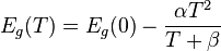 , where Eg(0), α and β are material constants.[2]
In a regular semiconductor crystal, the band gap is fixed owing to continuous energy states. In a quantum dot crystal, the band gap is size dependent and can be altered to produce a range of energies between the valence band and conduction band.[3] It is also known as quantum confinement effect.
Band gaps also depend on pressure. Band gaps can be either direct or indirect, depending on the electronic band structure.
Mathematical interpretation
Classically, the ratio of probabilities that two states with an energy difference ΔE will be occupied by an electron is given by the Boltzmann factor:

where:
- ΔE is the energy difference
- k is Boltzmann's constant
- T is temperature.
At the Fermi level (or chemical potential), the probability of a state being occupied is ½. If the Fermi level is in the middle of a band gap of 1 eV, this ratio is e−20 or about 2.0⋅10−9 at the room-temperature thermal energy of 25.9 meV.
Photovoltaic cells

The optical band gap (see below) determines what portion of the solar spectrum a photovoltaic cell absorbs.[4] A luminescent solar converter uses a luminescent medium to downconvert photons with energies above the band gap to photon energies closer to the band gap of the semiconductor comprising the solar cell.[5]
List of band gaps
Below are band gap values for some selected materials. For a comprehensive list of band gaps in semiconductors, see List of semiconductor materials.
| Group | Material | Symbol | Band gap (eV) @ 302K | Reference |
|---|---|---|---|---|
| IV | Diamond | C | 5.5 | [6] |
| IV | Silicon | Si | 1.11 | [7] |
| IV | Germanium | Ge | 0.67 | [7] |
| III–V | Gallium(III) nitride | GaN | 3.4 | [7] |
| III–V | Gallium(III) phosphide | GaP | 2.26 | [7] |
| III–V | Gallium(III) arsenide | GaAs | 1.43 | [7] |
| IV–V | Silicon nitride | Si3N4 | 5 | |
| IV–VI | Lead(II) sulfide | PbS | 0.37 | [7] |
| IV–VI | Silicon dioxide | SiO2 | 9 | [8] |
| Copper(I) oxide | Cu2O | 2.1 | [9] |
Optical versus electronic bandgap
In materials with a large exciton binding energy, it is possible for a photon to have just barely enough energy to create an exciton (bound electron–hole pair), but not enough energy to separate the electron and hole (which are electrically attracted to each other). In this situation, there is a distinction between "optical bandgap" and "electrical band gap" (or "transport gap"). The optical bandgap is the threshold for photons to be absorbed, while the transport gap is the threshold for creating an electron–hole pair that is not bound together. (The optical bandgap is at a lower energy than the transport gap.)
In almost all inorganic semiconductors, such as silicon, gallium arsenide, etc., there is very little interaction between electrons and holes (very small exciton binding energy), and therefore the optical and electronic bandgap are essentially identical, and the distinction between them is ignored. However, in some systems, including organic semiconductors, the distinction may be significant.
In photonics and phononics
In photonics band gaps or stop bands are ranges of photon frequencies where, if tunneling effects are neglected, no photons can be transmitted through a material. A material exhibiting this behaviour is known as a photonic crystal.
Similar physics applies to phonons in a phononic crystal.
Materials
List of electronics topics
- Electronics
- Bandgap voltage reference
- Condensed matter physics
- Direct and indirect bandgaps
- Electrical conduction
- Electron hole
- Field-effect transistor
- Photodiode
- Photoresistor
- Photovoltaics
- Solar cell
- Solid state physics
- Semiconductor
- Semiconductor devices
- Strongly correlated material
- Valence band
See also
- Wide bandgap semiconductors
- Band bending
- Spectral density
- Pseudogap
References
- ↑ H. Unlu (1992). "A Thermodynamic Model for Determining Pressure and Temperature Effects on the Bandgap Energies and other Properties of some Semiconductors". Solid State Electronics 35 (9): 1343–1352. Bibcode:1992SSEle..35.1343U. doi:10.1016/0038-1101(92)90170-H.
- ↑ Temperature dependence of the energy bandgap. Ece-www.colorado.edu. Retrieved on 2013-04-03.
- ↑ “Evident Technologies”. Evidenttech.com. Retrieved on 2013-04-03.
- ↑ Nanoscale Material Design. Nrel.gov. Retrieved on 2013-04-03.
- ↑ Nanocrystalline luminescent solar converters, 2004
- ↑ Kittel, Charles. Introduction to Solid State Physics, 7th Edition. Wiley.
- ↑ 7.0 7.1 7.2 7.3 7.4 7.5 Streetman, Ben G.; Sanjay Banerjee (2000). Solid State electronic Devices (5th ed.). New Jersey: Prentice Hall. p. 524. ISBN 0-13-025538-6.
- ↑ Vella, E.; Messina, F.; Cannas, M.; Boscaino, R. (2011). "Unraveling exciton dynamics in amorphous silicon dioxide: Interpretation of the optical features from 8 to 11 eV". Physical Review B 83: 174201. Bibcode:2011PhRvB..83q4201V. doi:10.1103/PhysRevB.83.174201.
- ↑ Baumeister, P.W. (1961). "Optical Absorption of Cuprous Oxide". Physical Review 121 (2): 359. Bibcode:1961PhRv..121..359B. doi:10.1103/PhysRev.121.359.
External links
- Direct Band Gap Energy Calculator
- Moriarty, Philip. "Energy Gap (and what makes glass transparent?)". Sixty Symbols. Brady Haran for the University of Nottingham.