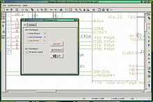
Schematic capture

Schematic capture or schematic entry is a step in the design cycle of electronic design automation (EDA) at which the electronic diagram, or electronic schematic of the designed electronic circuit is created by a designer. This is done interactively with the help of a schematic capture tool also known as schematic editor.
The circuit design is the very first step of actual design of an electronic circuit. Typically sketches are drawn on paper, and then entered into a computer using a schematic editor. Therefore schematic entry is said to be a front-end operation of several others in the design flow.
Despite the complexity of modern components – huge ball grid arrays and tiny passive components – schematic capture is easier today than it has been for many years. CAD software is easier to use and is available in full-featured expensive packages, very capable mid-range packages that sometimes have free versions and completely free versions that are either open source or directly linked to a printed circuit board fabrication company.
In past years, schematic diagrams with mostly discrete components were fairly readable. However, with the newer high pin-count parts and with the almost universal use of standard letter or A4 sized paper, schematics have become less so. Many times, there will be a single large part on a page with nothing but pin reference keys to connect it to other pages.
Readability levels can be enhanced by using buses and superbuses, related pins can be connected into a common bus and routed to other pages. Buses don't need to be just the traditional address or data bus directly linked pins. A bus grouping can also be used for related uses, such as all analog input or all communications related pin functions.
Other Considerations
After the circuit design is captured in a schematic, most EDA tools allow the design to be simulated.
Schematic capture involves not only entering the circuits into the CAD system, but also generally calls for decisions that may seem more appropriate for later in the design, such as package choice. Although you may be able to change the package later, many PCB CAD systems ask you to choose both the part and package when placing it into the schematic capture program.
This also brings into play such considerations as prototyping and assembly. In a high-volume assembly environment, there will be plenty of opportunities for DFM analysis. However, in a rapid prototyping environment such as at assembly houses specializing in low-volume/high-mix and quick turnaround times, the pick and place machines are programmed directly from the board layout files. Careful package selection during schematic capture will save time during the assembly and debug process.
With new parts, the CAD system may not have your chosen component in its parts library, so you may need to create the parts library yourself. Again, you may at the time not be overly concerned with the package, but careful creation of the part library will save time and risk later.
After the circuit design is captured in a schematic, then the PCB layout can begin.
Schematic Capture Tips
To make schematics easier to read there are a few tips that can increase organization and readability.
- Schematics should read left to right, just like a book. Generally, inputs on the left, outputs on the right.
- Naming signals / nets will dramatically increase the readability and traceability of your schematics. It will be a great help during the pcb design phase of your project.
- No 4-way ties. A 4-way tie can cause confusion and should be avoided at all times (This 'tip' is often contended among design professionals).
- Break the schematic into logical building blocks. This is easily accomplished with multiple pages, each having a dedicated functionality.
- Use all capital letters as much as possible, especially for small text such as net names. This improves legibility, and is required by most drafting standards.
- To maximize portability, net names should consist of letters, numbers, and underscores. Use of characters such as spaces, pluses or minuses, or case sensitive names (i.e. two or more names who only differ in case) is discouraged, as it can cause subtle problems when exporting a netlist for simulation or layout. For example, net names in Verilog cannot have spaces; a netlist export tool would have to "escape" these characters to allow a Verilog simulation, which could lead to confusion if there are later errors referencing these nets.
See also
| Wikibooks has a book on the topic of: Robotics: Design Basics: Design software |
| The Wikibook Practical Electronics has a page on the topic of: PCB Layout |
Individual products
- Altium – Providers of Altium Designer (formerly Protel) and P-CAD (retired June 30, 2008).
- Autotrax – EDA/DEX is a Windows XP/Vista/7 schematic capture / PCB design layout program with built-in Spice simulator and 3D part and board visualization.
- DipTrace – mid-range Schematic Capture and PCB Layout software that has a free version.
- Edwinxp – Totally Integrated Schematic Capture, Simulation and PCB design software.
- Electronics Workbench – Schematic Capture, Simulation and PCB design software suite.
- Multisim – Schematic Capture and SPICE Simulation software.
- CadSoft EAGLE – Very capable mid-range Schematic Capture and PCB Layout software that has a free version.
- KiCad – open source schematic capture and PCB design software suite
- OrCAD – Full-featured commercial Schematic Capture and PCB layout.
- TARGET 3001! – mid-range Schematic Capture software that has a free version.
- gEDA – open source schematic capture using gschem, simulation, and PCB design software suite
- The Electric VLSI Design System
- PADs – Full-featured commercial Schematic Capture and PCB layout from Mentor Graphics.
References
- Pratt, Gary; Jarrett, Jay (August 6, 2001), "Top-Down Design Methods Bring Back The Useful Schematic Diagram", Electronic Design 49 (16): 69–unknown, ISSN 0013-4872, ED Online ID #3784.