Inverter (logic gate)
| INPUT | OUTPUT |
| A | NOT A |
| 0 | 1 |
| 1 | 0 |

In digital logic, an inverter or NOT gate is a logic gate which implements logical negation. The truth table is shown on the right.
Electronic implementation
-
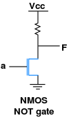
NMOS inverter
-
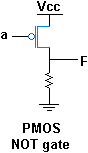
PMOS inverter
-
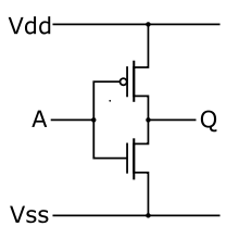
Static CMOS inverter
-

NPN transistor–transistor logic inverter
-

Saturated-load NMOS inverter
-

NPN resistor–transistor logic inverter

An inverter circuit outputs a voltage representing the opposite logic-level to its input. Inverters can be constructed using a single NMOS transistor or a single PMOS transistor coupled with a resistor. Since this 'resistive-drain' approach uses only a single type of transistor, it can be fabricated at low cost. However, because current flows through the resistor in one of the two states, the resistive-drain configuration is disadvantaged for power consumption and processing speed. Alternatively, inverters can be constructed using two complementary transistors in a CMOS configuration. This configuration greatly reduces power consumption since one of the transistors is always off in both logic states. Processing speed can also be improved due to the relatively low resistance compared to the NMOS-only or PMOS-only type devices. Inverters can also be constructed with bipolar junction transistors (BJT) in either a resistor-transistor logic (RTL) or a transistor-transistor logic (TTL) configuration.
Digital electronics circuits operate at fixed voltage levels corresponding to a logical 0 or 1 (see binary). An inverter circuit serves as the basic logic gate to swap between those two voltage levels. Implementation determines the actual voltage, but common levels include (0, +5V) for TTL circuits.
Digital building block

The digital inverter is considered the base building block for all digital electronics. Memory (1-bit register) is built as a latch by feeding the output of two inverters to each other's input. Multiplexers, decoders, state machines, and other sophisticated digital devices all rely on the basic inverter.
The hex inverter is an integrated circuit that contains six (hexa-) inverters. For example, the 7404 TTL chip which has 14 pins and the 4049 CMOS chip which has 16 pins, 2 of which are used for power/referencing, and 12 of which are used by the inputs and outputs of the six inverters (the 4049 has 2 pins with no connection).
Performance measurement
Digital inverter quality is often measured using the voltage transfer curve (VTC), which is a plot of output vs. input voltage. From such a graph, device parameters including noise tolerance, gain, and operating logic levels can be obtained.
Ideally, the VTC appears as an inverted step function – this would indicate precise switching between on and off – but in real devices, a gradual transition region exists. The VTC indicates that for low input voltage, the circuit outputs high voltage; for high input, the output tapers off towards the low level. The slope of this transition region is a measure of quality – steep (close to infinity) slopes yield precise switching.
The tolerance to noise can be measured by comparing the minimum input to the maximum output for each region of operation (on / off).
See also
- Controlled NOT gate
- AND gate
- OR gate
- NAND gate
- NOR gate
- XOR gate
- XNOR gate
- Boolean algebra (logic)
- Logic gates