Indium gallium arsenide
Indium gallium arsenide (InGaAs), also called gallium indium arsenide, is a common name for a family of chemical compounds of three chemical elements, indium, gallium, and arsenic. Indium and gallium are both boron group elements, often called "group III", while arsenic is a pnictogen or "group V" element. In semiconductor physics, compounds of elements in these groups are often called "III-V" compounds. Because they belong to the same group, indium and gallium play similar roles in chemical bonding, and InGaAs is often regarded as an alloy of gallium arsenide and indium arsenide, with its properties being intermediate between the two and depending on the proportion of gallium to indium. Under typical conditions, InGaAs is a semiconductor, and it is especially significant in optoelectronics technology, for which reason it has been extensively studied.
Nomenclature
Indium gallium arsenide is a popular designation for gallium-indium arsenide (GaInAs). InGaAs is a direct bandgap, pseudo-binary alloy composed of two III-V semiconducting materials: (GaAs)X and (InAs)1-X. The alloy is miscible over the entire compositional range from GaAs (bandgap = 1.42 eV at 300 K) to InAs (bandgap = 0.34 eV at 300 K).[4] GaXIn1-XAs is a technologically important semiconductor widely exploited in optical communications, photovoltaics, sensor and laser applications.
According to standards of the IUPAC[5] The preferred nomenclature for the alloy is In1-XGaXAs where the group-III elements appear in order of increasing atomic number, as in the related alloy system AlXGa1-XAs.[6]
Electronic and optical properties: measurements on polycrystalline samples

Indium Gallium arsenide has a lattice parameter that increases linearly with the concentration of InAs in the alloy.[7] The liquid-solid phase diagram[8] shows that during solidification from a solution containing GaAs and InAs, GaAs is taken up at a much higher rate than InAs, depleting the solution of GaAs. During growth from solution, the composition of first material to solidify is rich in GaAs while the last material to solidify is richer in InAs. This feature has been exploited to produce ingots of InGaAs with graded composition along the length of the ingot. However, the strain introduced by the changing lattice constant causes the ingot to be polycrystalline, and limiting the characterization to a few parameters, with uncertainty due to the continuous compositional grading in the materials.

J.C. Woolley and his students at the University of Ottawa used this approach in the 1960s to characterise the optical properties of a large number of III-V pseudo binary alloy systems. Although the polycrystalline nature of the samples used made them unsuitable for device applications, the experimental results and analysis do provide a comprehensive overview of the potential of III-V semiconductor alloys. While more precise measurements have been obtained on single-crystal samples, such as the case of epitaxial InGaAs grown lattice-matched on InP, Woolley’s results represent the best body of data today for alloy compositions that cannot by synthesized as single-crystal epitaxial films for lack of the appropriate substrate.
The optical and mechanical properties of InGaAs can be varied by changing the ratio of InAs and GaAs, In1-xGaxAs.[9] The GaInAs device is normally grown on an indium phosphide (InP) substrate. In order to match the lattice constant of InP and avoid mechanical strain, In0.53Ga0.47As is used. This composition has a cut-off wavelength of 1.68 μm at 295 K.
By increasing the mole fraction of InAs further compared to GaAs it is possible to extend the cut-off wavelength up to about 2.6 µm. In that case special measures have to be taken to avoid mechanical strain from differences in lattice constants.
GaAs is lattice mismatched to Ge by 0.08%. With the addition of 1.5% In to the alloy, InGaAs, becomes perfectly latticed matched to Ge. The complete elimination of film stress reduces the defect densities of the epi InGaAs layer compared to straight GaAs.

Properties of single crystal GaInAs
Single crystal GaInAs
Single crystal epitaxial films of GaInAs can be deposited on a single crystal substrate of III-V semiconductor having a lattice parameter close to that of the specific gallium indium arsenide alloy to be synthesized. There are three substrates that can be used: GaAs, InAs and InP. A good match between the lattice constants of the film and substrate is required to maintain single crystal properties and this limitation permits small variation in composition on the order of a few per cent. Therefore the properties of epitaxial films of GaInAs alloys grown on GaAs are very similar to GaAs and those grown on InAs are very similar to InAs, because lattice mismatch strain does not generally permit significant deviation of the composition from the pure binary substrate
Ga0.47In0.53As is the alloy whose lattice parameter matches that of InP at 295 K. Yoshikazu Takeda was the first to grow epitaxial films of GaInAs lattice-matched on InP substrates.[10] Pearsall and Hopson determined the phase diagram and procedures for epitaxial growth of Ga0.47In0.53As.[11]
GaInAs lattice-matched to InP is a semiconductor with properties quite different from GaAs, InAs or InP. It has an energy band gap of 0.75 eV, an electron effective mass of 0.041 and an electron mobility close to 10,000 cm2·V−1·s−1 at room temperature, all of which are more favorable for many electronic and photonic device applications when compared to GaAs, InP or even Si.[12]
| Property | Value at 295 K | Reference |
|---|---|---|
| Lattice Parameter | 5.869 Å | [13] |
| Band Gap | 0.75 eV | [12] |
| Electron effective mass | 0.041 | [14] |
| Light-hole effective mass | 0.051 | [15] |
| Electron mobility | 10,000 cm2·V−1·s−1 | [2] |
| Hole mobility | 250 cm2·V−1·s−1 | [2] |
FCC lattice parameter
Like most materials, the lattice parameter of GaInAs is a function of temperature. The measured coefficient of thermal expansion (see ref. n°9) is 5.66×10⁻⁶ K−1. This is significantly larger than the coefficient for InP which is 4.56×10⁻⁶ K−1. A film that is exactly lattice-matched to InP at room temperature is typically grown at 650 °C with a lattice mismatch of +6.5×10⁻⁴. Such a film has a mole fraction of GaAs = 0.47. To obtain lattice matching at the growth temperature, it is necessary to increase the GaAs mole fraction to 0.48.
Bandgap energy
The bandgap energy of GaInAs can be determined from the peak in the photoluminescence spectrum, provided that the total impurity and defect concentration is less than 5×1016 cm−3. The bandgap energy depends on temperature and increases as the temperature decreases, as can be seen in Fig. 3 for both n-type and p-type samples. The bandgap energy at room temperature is 0.75 eV, and lies between that of Ge and Si. By coincidence the bandgap of GaInAs is perfectly placed for photodetector and laser applications for the long-wavelength transmission window, (the C-band and L-band) for fiber-optic communications.
Effective mass
The electron effective mass of GaInAs m*/m° = 0.041 [14] is the smallest for any semiconductor material with an energy bandgap greater than 0.5 eV. The effective mass is determined from the curvature of the energy-momentum relationship: stronger curvature translates into lower effective mass and a larger radius of delocalization. In practical terms, a low effective mass leads directly to high carrier mobility, favoring higher speed of transport, and greater current carrying capacity. A lower carrier effective mass also favors increased tunneling current, a direct result of delocalization.
There are two types of charge carriers in the valence band: light holes: m*/m° = 0.051 [15] and heavy holes: m*/m° = 0.2.[16] The electrical and optical properties of the valence band are dominated by the heavy holes, because the density of these states is much greater than that for light holes. This is also reflected in the mobility of holes at 295 K, which is a factor of 40 lower than that for electrons.

Mobility of electrons and holes
Electron mobility and hole mobility are key parameters for design and performance of electronic devices. Measured carrier mobilities for electrons and holes are shown in Figure 4.
The mobility of carriers in Ga0.47In0.53As is usual in two regards:
- The very high value of electron mobility
- The unusually large ratio of electron to hole mobility.
The room temperature electron mobility for reasonably pure samples of Ga0.47In0.53As approaches 104 cm2·V−1·s−1, which is the largest of any technologically important semiconductor, although significantly less than that for graphene.
The mobility is proportional to the carrier conductivity. As the mobility increases, so does the current-carrying capacity of transistors. A higher mobility shortens the response time of photodetectors. A larger mobility reduces series resistance, and this improves the efficiency of solar cells and reduces noise and power consumption of transistors.
The minority carrier diffusion constant is directly proportional to carrier mobility. The room temperature diffusion constant for electrons at 250 cm2·s−1 is significantly larger than that of Si, GaAs, Ge or InP, and determines the ultra-fast response of Ga0.47In0.53As photodetectors.
The ratio of electron to hole mobility is the largest of currently-used semiconductors. This ratio determines the gain of photoconductive detectors.

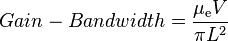
The gain-bandwidth product depends on the electron mobility alone.[17] The relatively large gain-bandwidth product in tandem with the spectral response in the near infra-red positions Ga0.47In0.53As as an ideal material for night vision imaging components.
Applications

Photodetectors
The principal application of GaInAs is as an infrared detector. The spectral response of a GaInAs photodiode is shown in Figure 5. GaInAs photodiodes are the preferred choice in the wavelength range of 1.1 µm to 1.7 µm. For example compared to photodiodes made from Ge, GaInAs photodiodes have faster time response, higher quantum efficiency and lower dark current for the same sensor area.[18] GaInAs photodiodes were invented in 1977 by Pearsall.[19]
Avalanche photodiodes offer the advantage of additional gain at the expense of response time. These devices are especially useful for detection of single photons in applications such as quantum key distribution where response time is not critical. Avalanche photodetectors require a special structure to reduce reverse leakage current due to tunnelling. The first practical avalanche photodiodes were designed and demonstrated by Nishida in 1979.[20]
In 1980, Pearsall developed a photodiode design that exploits the uniquely short diffusion time of high mobility of electrons in GaInAs, leading to an ultrafast response time.[21][22] Fifteen years later in 1998, this structure was further developed and named the UTC, or uni-travelling carrier photodiode.[23]
Other important innovations include the integrated photodiode – FET receiver[24] and the engineering of GaInAs focal-plane arrays.[25]
Transistors
HEMT devices using InGaAs channels are one of the fastest types of transistor.[26]
GaInAs is also a popular material in triple-junction photovoltaics, and also for thermophotovoltaic power generation. GaInAs can be used as a laser medium. Devices have been constructed operating at wavelengths of 905 nm, 980 nm, 1060 nm, and 1300 nm. InGaAs quantum dots on GaAs have also been studied as lasers.
In0.015Ga0.985As can be used as an intermediate band-gap junction in multi-junction photovoltaic cells with a perfect lattice match to Ge. The perfect lattice match to Ge reduces defect density, improving cell efficiency.
MIT researchers created the smallest transistor ever built from a material other than silicon. The metal-oxide semiconductor field-effect transistor (MOSFET) is 22 nanometers long.[27]
Safety and toxicity aspects
The synthesis of GaInAs, like that of GaAs most often involves the use of arsine (AsH3), an extremely toxic gas. Synthesis of InP likewise most often involves phosphine (PH3). Inhalation of these gases neutralizes oxygen absorption by the bloodstream, and can be fatal within a few minutes if the toxic dose levels are exceeded. Safe handling of these materials involves using a sensitive toxic gas detection system and self-contained breathing apparatus. The environment, health and safety aspects of indium gallium arsenide sources (such as trimethylgallium, trimethylindium and arsine) and industrial hygiene monitoring studies of standard MOVPE sources have been reported recently in a review.[28]
Once GaInAs is deposited as a thin film on a substrate, it is basically inert, being resistant to abrasion, sublimation or dissolution by common solvents like water, alcohols or acetones. In device form the volume of the GaInAs is usually less than 1000 µm3, and can be neglected compared to the volume of the supporting substrate, InP or GaAs. For this reason, toxicology studies have first focussed on the properties of these substrates. A detailed toxicology study of GaAs has been carried out by the NIH in 2000.[29] a summary of studies concerning GaAs and InP has been published by the World Health Organization's International Agency for Research on Cancer.[30] These two works contain the most recent understanding of hazards presented by long-term exposure to GaAs or InP.
REACH (Registration, Evaluation, Authorisation and Restriction of Chemicals) is a European initiative to classify and regulate all materials that are used, or produced (even as waste) in manufacturing. REACH considers only 3 toxic classes: Carcinogenic, Reproductive, and mutation capacities of these materials. While this is a vast task, the existence of a professional toxicological studies on GaAs and InP moved these two substances to the head of the queue for classification by REACH.
The REACH classification procedure consists of 2 basic phases. In phase 1 the hazards intrinsic to the material are determined, without any consideration of how the material might be used or encountered in the work place or by a consumer. In phase 2 the risk of harmful exposure is taken into account along with procedures that can mitigate exposure. Both GaAs and InP are being considered in phase 1 at the present time. The principal risk of exposure occurs during substrate preparation where grinding and polishing generate micron-size particles of GaAs and InP. Similar concerns apply to wafer dicing to make individual devices. This particle dust can be absorbed by animals by breathing or ingested. The increased ratio of surface area to volume for such particles increases their chemical reactivity.
The toxicology studies referenced here are based on experiments where rats and mice are made to breathe air containing GaAs or InP dust. At present there are no studies of a comparable rigor to test the effects of ingesting GaAs or InP dust in a liquid slurry.
The principal observations of the NIH study are: 1. Under the conditions of these 2-year inhalation studies, there was no evidence of carcinogenic activity of gallium arsenide in male F344/N rats exposed to 0.01, 0.1, or 1.0 mg/m3. 2. There was clear evidence of carcinogenic activity in female F344/N rats 3. There was no evidence of carcinogenic activity in male or female B6C3F1 mice exposed to 0.1, 0.5, or 1.0 mg/m3.
The WHO study considered and analyzed the results of the NIH toxicology study. Their conclusions are: 1. There is inadequate evidence in humans for the carcinogenicity of gallium arsenide. 2. There is limited evidence in experimental animals for the carcinogenicity of gallium arsenide. 3. The gallium moiety may be responsible for lung cancers observed in female rats
The REACH procedure, acting under the principle of precaution, interprets "inadequate evidence for carcenogenicity" as "possible carcinogen". As as result, ECHA classified InP in 2010 as a carcinogen and reproductive toxin:
- Classification & labelling in accordance with Directive 67/548/EEC
- Classification: Carc. Cat. 2; R45
- Repr. Cat. 3; R62
and ECHA classified GaAs in 2010 as a carcinogen and reproductive toxin:
- Classification & labelling in accordance with Directive 67/548/EEC:
- Classification3: Carc. Cat. 1; R45
- Repro. Cat. 2; R60
Further details and documentation are made available by the European Chemicals Agency, ECHA [31] who carried out the classifications.
See also
References
- ↑ T.P. Pearsall, L. Eaves and J.C. Portal, "Photoluminescence and Impurity Concentration in GaInAsP Lattice-matched to InP", J. Appl. Phys. 52 pp.1037-1047 (1983).
- ↑ 2.0 2.1 2.2 T.P. Pearsall and J.P. Hirtz, J. Cryst. Growth 54, pp. 127-131 (1981)
- ↑ T.P. Pearsall, "InGaAs Photodetectors" in Properties of Lattice-Matched and Strained Indium Gallium Arsenide, ed P.Bhattacharya, (London, IEE Press, 1993) pp267-77.
- ↑ John C. Woolley, Mathew B. Thomas, Alan G. Thompson. "Optical energy gap variation in GaxIn1−x As alloys". Nrcresearchpress.com. Retrieved 2013-12-02.
- ↑ "International Union of Pure and Applied Chemistry: Home". IUPAC. Retrieved 2013-09-22.
- ↑ Aluminum gallium arsenide
- ↑ John W. Wagner. "Preparation and Properties of Bulk In1 − x Ga x As Alloys : SOLID STATE SCIENCE - Technical Papers". Jes.ecsdl.org. Retrieved 2013-12-02.
- ↑
- ↑ "Technology: What is InGaAs?". Sensorsinc.com. Retrieved 2013-12-02.
- ↑ "Scitation: Electron mobility and energy gap of In0.53Ga0.47As on InP substrate". Jap.aip.org. Retrieved 2013-12-02.
- ↑ "Scitation: Journal of Applied Physics". Jap.aip.org. 2006-06-16. Retrieved 2013-12-02.
- ↑ 12.0 12.1 "IEEE Xplore - Ga0.47In0.53As: A ternary semiconductor for photodetector applications". Ieeexplore.ieee.org. doi:10.1109/JQE.1980.1070557. Retrieved 2013-12-02.
- ↑ T.P. Pearsall, R. Bisaro, R. Ansel and P. Merenda, Appl. Phys. Lett. 32, pp. 497-9 (1978)
- ↑ 14.0 14.1 R.J. Nicholas, J.C. Portal, C.Houlbert, P.Perrier and T.P. Pearsall, Appl. Phys. Lett 34, pp. 492-4 (1979)
- ↑ 15.0 15.1 Claudine Hermann and T.P. Pearsall, Appl. Phys. Lett 38, pp. 450-2 (1981)
- ↑ S.Y. Lin, C.T. Liu D.C. Tsui, E.D. Jones and L.R. Dawson, Appl.Phys. Lett. 55, Pp.666-8 (1989)
- ↑ Thomas P. Pearsall Photonics Essentials, 2nd Edition: McGraw-Hill, New York; NY 2010, ISBN 978-0-07-162935-5
- ↑ T.P. Pearsall and M.A. Pollack, Semiconductors and Semimetals, vol 22D, Ed; W.T. Tsang, (New York, Academic Press, 1985)
- ↑ T.P. Pearsall and R.W. Hopson, Jr, Electronic Materials Conference, Cornell University, 1977, published in J. Electron. Mat. 7, pp.133-146, (1978)
- ↑ K. Nishida, K. Taguchi, and Y. Matsumoto, Appl. Phys. Lett. 35, pp.251-3, 1979
- ↑ T.P. Pearsall and M. Piskorski A. Brochet, and J; Chevrier, IEEE J. Quant Electron QE-17, pp255-9, 1981
- ↑ T.P. Pearsall, R.A. Logan C.G. Bethea, Electron Lett, 19, pp 611-612 1983
- ↑ N. Shimizu, N. Watanabe, T. Furuta, a,d T; Ishibashi, IEEE Photon. Tech. Letters, 10, 412-4, 1998
- ↑ R.F. Leheny, R.E. Nahory, M.A. Pollack, A.A. Ballman, E.D. Beebe, J.C. DeWinter, and R.J. Martin, Electron./ Lett 16, pp353-5 1980
- ↑ "Sensors Unlimited - InGaAs Near and Short Wave Infrared (SWIR) Cameras, Arrays, and Photodiodes". Sensorsinc.com. Retrieved 2013-09-22.
- ↑
- ↑ Layne Nelson (2012-12-14). "Indium gallium arsenide transistor could boost microchip performance". Gizmag.com. Retrieved 2013-09-22.
- ↑ Shenai-Khatkhate, D.V. et al. (2004). "Environment, health and safety issues for sources used in MOVPE growth of compound semiconductors". Journal of Crystal Growth 272 (1–4): 816–821. Bibcode:2004JCrGr.272..816S. doi:10.1016/j.jcrysgro.2004.09.007.
- ↑ "NTP Technical Report on the Toxicology and Carcinogenesis Studies of Gallium Arsenide". Ntp.niehs.nih.gov. Retrieved 2013-09-22.
- ↑ "IARC Monographs on the Evaluation of Carcinogenic Risks to Humans". Monographs.iarc.fr. Retrieved 2013-09-22.
- ↑ "Homepage - ECHA". Echa.europa.eu. Retrieved 2013-09-22.
External links
- NSM data archive at the Ioffe Institute, St. Petersburg, Russia