Field emission microscopy
Field emission microscopy (FEM) is an analytical technique used in materials science to investigate molecular surface structures and their electronic properties.[1] Invented by Erwin Wilhelm Müller in 1936, the FEM was one of the first surface analysis instruments that approached near-atomic resolution.
Introduction
Microscopy techniques are used to produce real space magnified images of a surface showing what it looks like. In general microscopy information concerns surface crystallography (i.e. how the atoms are arranged at the surface), surface morphology (i.e. the shape and size of topographic features making the surface), and surface composition (the elements and compounds the surface is composed of).
Field emission microscopy (FEM) was invented by Erwin Müller in 1936. In FEM, the phenomenon of field electron emission was used to obtain an image on the detector on the basis of the difference in work function of the various crystallographic planes on the surface.
Design
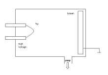
A Field Emission Microscope consists of a metallic sample in the form of a sharp tip and a conducting fluorescent screen enclosed in ultrahigh vacuum. The tip radius used is typically of the order of 100 nm. It is composed of a metal with a high melting point, such as tungsten.[2] The sample is held at a large negative potential (1-10 kV) relative to the fluorescent screen. This gives the electric field near the tip apex to be the order of 1010 V/m which is high enough for field emission of electrons to take place. Fig.1 shows the experimental set up for FEM.

The field emitted electrons travel along the field lines and produce bright and dark patches on the fluorescent screen giving a one-to-one correspondence with the crystal planes of the hemispherical emitter. The emission current varies strongly with the local work function in accordance with the Fowler-Nordheim equation; hence, the FEM image displays the projected work function map of the emitter surface. The closely packed faces have higher work functions than atomically rough regions and thus they show up in the image as dark spots on the brighter background. In short, the work function anisotropy of the crystal planes is mapped onto the screen as intensity variations.
The magnification is given by the ratio  , where
  is the tip apex radius and
  is the tip-screen distance. Linear magnifications of about 105 to 106 are attained. The spatial resolution of this technique is of the order of 2 nm and is limited by the momentum of the emitted electrons parallel to the tip surface, which is of the order of the Fermi velocity of the electron in metal.
It is possible to set up an FEM with a probe hole in the phosphor screen and a Faraday cup collector behind it to collect the current emitted from a single plane. This technique allows the measurement of the variation of work function with orientation for a wide variety of orientations on a single sample. The FEM has also been used to study adsorption and surface diffusion processes, making use of the work function change associated with the adsorption process.
Field emission requires a very good vacuum, and often, even in ultra high vacuum (UHV), emission is not due to the clean surface. A typical field emitter needs to be ‘flashed’ to clean it, usually by passing a current through a loop on which it is mounted. After flashing the emission current is high but unstable. The current decays with time and in the process becomes more stable due to the contamination of the tip, either from the vacuum, or more often from diffusion of adsorbed surface species to the tip. Thus the real nature of the FEM tips during use is somewhat unknown.
Application of FEM is limited by the materials which can be fabricated in the shape of a sharp tip, can be used in a UHV environment, and can tolerate the high electrostatic fields. For these reasons, refractory metals with high melting temperature (for e.g. W, Mo, Pt, Ir) are conventional objects for FEM experiments.
See also
- Atom Probe
- Electron microscope
- Field ion microscope
- List of surface analysis methods
References
- ↑ "Intro to Field Emission". Field Emission / Ion Microscopy Laboratory, Purdue University, Dept. of Physics. Retrieved 2007-05-10.
- ↑ Stranks, D. R.; M. L. Heffernan, K. C. Lee Dow, P. T. McTigue, G. R. A. Withers (1970). Chemistry: A structural view. Carlton, Victoria: Melbourne University Press. p. 5. ISBN 0-522-83988-6.
- 2. K.Oura, V.G.Lifshits, A.ASaranin, A.V.Zotov and M.Katayama, Surface Science – An Introduction, (Springer-Verlag Berlin Heidelberg 2003).
- 3. John B. Hudson, Surface Science – An Introduction, (BUTTERWORTH-Heinemann 1992).