Banyan switch
In electronics, a banyan switch is a complex crossover switch used in electrical or optical switches.
It is named for its resemblance to the roots of the banyan tree which cross over in complex patterns. Logical banyan switches are used in logic or signal pathways to crossover switching of signals onto new pathways.
They can be mechanical Microelectromechanical systems, electrical or optical NLO. Their complexity depends on the topology of the individual switches in a switch matrix (how wide it is by how many 'plies' or layers of switches it takes), to implement a desired crossover logic.
Design
Typical crossover matrices follow this formula: an N×N banyan switch uses (N/2) log2 N elements. Other formulas are used for differing number of crossover layers, and scaling is possible, but becomes very large and complex with large N×N arrays. CAD and AI can be used to take the drudgery out of creating these designs. A banyan network is implemented by interconnecting 2×2 switching networks in multiple and recursive stages.
The switches are measured by how many stages, and how many up/down sorters and crosspoints they have. Switches often have buffers built-in for faster switching.
A typical switch may have:
- A 2×2 and 4×4 down sorter
- Followed by an 8×8 up sorter
- Followed by a 2×2 crosspoint banyan switch network
This results in 3 level sorting for a 3 stage banyan network switch.
A simple example

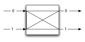
Consider a 2×2 banyan switch, which requires (2/2) log2 2 = 1 switching element. This switch takes two inputs, numbered 0 and 1, and two outputs, numbered 0 and 1. Every packet that comes in has a header that contains one bit indicating what its destination is (either 0 or 1). If the switch reads the bit and it has value 0, it sends the packet to its higher output (which is 0 in this case), and to its lower output if the routing bit is one. By connecting these switching elements in series and parallel it is possible therefore, to route packets in more complicated ways depending on the desired routes to establish.
Future directions and further information
The future is moving to larger arrays of inputs and outputs needed in a very small space. See wafer fabrication and VLAs.
See also
- Crossover switches
- Crossbar switches
- Clos network a non blocking crossover switch that needs fewer than N² switches
- Nonblocking minimal spanning switch and signal switching.
- Optical computer