Threshold voltage
The threshold voltage of a MOSFET is usually defined as the gate voltage where an inversion layer forms at the interface between the insulating layer (oxide) and the substrate (body) of the transistor. The purpose of the inversion layer's forming is to allow the flow of electrons through the gate-source junction. The creation of this layer is described next.
In an n-MOSFET the substrate of the transistor is composed of p-type silicon (see doping (semiconductor)), which has positively charged mobile holes as carriers. When a positive voltage is applied on the gate, an electric field causes the holes to be repelled from the interface, creating a depletion region containing immobile negatively charged acceptor ions. A further increase in the gate voltage eventually causes electrons to appear at the interface, in what is called an inversion layer, or channel. Historically the gate voltage at which the electron density at the interface is the same as the hole density in the neutral bulk material is called the threshold voltage. Practically speaking the threshold voltage is the voltage at which there are sufficient electrons in the inversion layer to make a low resistance conducting path between the MOSFET source and drain.
In the figures, the source (left side) and drain (right side) are labeled n+ to indicate heavily doped (blue) n-regions. The depletion layer dopant is labeled NA− to indicate that the ions in the (pink) depletion layer are negatively charged and there are very few holes. In the (red) bulk the number of holes p = NA making the bulk charge neutral.
If the gate voltage is below the threshold voltage (top figure), the transistor is turned off and ideally there is no current from the drain to the source of the transistor. In fact, there is a current even for gate biases below threshold (subthreshold leakage) current, although it is small and varies exponentially with gate bias.
If the gate voltage is above the threshold voltage (lower figure), the transistor is turned on, due to there being many electrons in the channel at the oxide-silicon interface, creating a low-resistance channel where charge can flow from drain to source. For voltages significantly above threshold, this situation is called strong inversion. The channel is tapered when VD > 0 because the voltage drop due to the current in the resistive channel reduces the oxide field supporting the channel as the drain is approached.
In modern devices the threshold voltage is a much less clear-cut parameter subject to variation with the biases applied to the device; see drain induced barrier lowering.
Contents |
Body effect
The body effect describes the changes in the threshold voltage by the change in  , the source-bulk voltage. Since the body influences the threshold voltage (when it is not tied to the source), it can be thought of as a second gate, and is sometimes referred to as the "back gate"; the body effect is sometimes called the "back-gate effect".[1]
For an enhancement mode, n-mos MOSFET body effect upon threshold voltage is computed according to the Shichman-Hodges model [2] (accurate for very old technology) using the following equation.

where  is the threshold voltage when substrate bias is present, is the source-to-body substrate bias,
  is the surface potential, and
  is threshold voltage for zero substrate bias,
 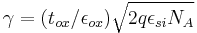 is the body effect parameter,
  is oxide thickness,
  is oxide permitivity,
  is the permitivity of silicon,
  is a doping concentration,
  is the charge of an electron.
Dependence on oxide thickness
In a given technology node, such as the 90 nanometer CMOS process, threshold voltage depends on the choice of oxide and on oxide thickness. Using the body formulas above, is directly proportional to  , and
, and  , which is the parameter for oxide thickness.
Thus, the thinner the oxide thickness, the lower the threshold voltage. While this may seem to be an improvement, it is not without cost; for the thinner the oxide thickness, the higher the subthreshold leakage current flowing through the device will be. Consequently, the design specification for 90 nanometer gate oxide thickness was set at 1 nanometer to control the leakage current.[3] This kind of tunneling, called Fowler-Nordheim Tunneling.[4]
where  and
and  are constants and
  is the electric field across the gate oxide.
Before scaling the design features down to 90 nanometers, a dual oxide approach for creating the oxide thickness was a common solution to this issue. With a 90 nanometer process technology, a triple oxide approach has been adopted in some cases.[5] One standard thin oxide is used for most transistors, another for I/O driver cells, and a third for memory and pass transistor cells. These differences are based purely on the characteristics of oxide thickness on threshold voltage of CMOS technologies.
Dependence on temperature
As with the case of oxide thickness affecting threshold voltage, temperature has an effect on the threshold voltage of a CMOS device. Expanding on part of the equation in the body effect section
where  is Boltzmann's constant,
  is Temperature, is the charge of an electron, is a doping parameter and
  is the intrinsic doping parameter for the substrate.
We see that the surface potential has a direct relationship with the temperature. Looking above, that while the threshold voltage does not have a direct relationship but is not independent of the effects. On average this variation is between −4 mV/°C and −2 mV/°C depending on doping level.[6] For a change of 30 °C this results in significant variation from the 500mV design parameter commonly used for the 90 nanometer technology node.
References
- ^ Marco Delaurenti, PhD dissertation, Design and optimization techniques of high-speed VLSI circuits (1999))[1]
- ^ NanoDotTek Report NDT14-08-2007, 12 August 2007
- ^ Sugii, Watanabe and Sugatani. Transistor Design for 90-nm Generation and Beyond. (2002) [2]
- ^ S. M. Sze, Physics of Semiconductor Devices, Second Edition, New York: Wiley and Sons, 1981, pp. 496–504.
- ^ Anil Telikepalli, Xilinx Inc, Power considerations in designing with 90 nm FPGAs (2005))[3]
- ^ Weste and Eshraghian, Principles of CMOS VLSI Design : a systems perspective, Second Edition, (1993) pp.48 ISBN 0-201-53376-6
External links
- Online lecture on: Threshold Voltage and MOSFET Capacitances by Dr. Lundstrom