Sallen–Key topology
The Sallen–Key topology is an electronic filter topology used to implement second-order active filters that is particularly valued for its simplicity.[1] It is a degenerate form of a voltage-controlled voltage-source (VCVS) filter topology. A VCVS filter uses a super-unity-gain voltage amplifier with practically infinite input impedance and zero output impedance to implement a 2-pole (12 dB/octave) low-pass, high-pass, or bandpass response. The super-unity-gain amplifier allows for very high Q factor and passband gain without the use of inductors. A Sallen–Key filter is a variation on a VCVS filter that uses a unity-gain amplifier (i.e., a pure buffer amplifier with 0 dB gain). It was introduced by R.P. Sallen and E. L. Key of MIT Lincoln Laboratory in 1955.[2]
Because of its high input impedance and easily selectable gain, an operational amplifier in a conventional non-inverting configuration is often used in VCVS implementations. Implementations of Sallen–Key filters often use an operational amplifier configured as a voltage follower; however, emitter or source followers are other common choices for the buffer amplifier.
VCVS filters are relatively resilient to component tolerance, but obtaining high Q factor may require extreme component value spread or high amplifier gain.[1] Higher-order filters can be obtained by cascading two or more stages.
Contents |
Generic Sallen–Key topology
The generic unity-gain Sallen–Key filter topology implemented with a unity-gain operational amplifier is shown in Figure 1. The following analysis is based on the assumption that the operational amplifier is ideal.
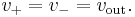
Because the operational amplifier (OA) is in a negative-feedback configuration, its v+ and v- inputs must match (i.e., v+ = v-). However, the inverting input v- is connected directly to the output vout, and so

By Kirchhoff's current law (KCL) applied at the vx node,
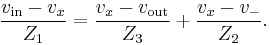

By combining Equations (1) and (2),
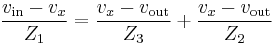
Applying Equation (1) and KCL at the OA's non-inverting input v+ gives
which means that

Combining Equations (2) and (3) gives
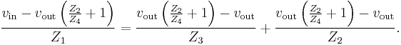

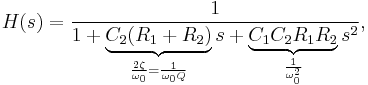
Rearranging Equation (4) gives the transfer function

which typically describes a second-order LTI system.
Interpretation
If the  component were connected to ground, the filter would be a voltage divider composed of the
  and components cascaded with another voltage divider composed of the
  and
and  components. The buffer bootstraps the "bottom" of the component to the output of the filter, which will improve upon the simple two divider case. This interpretation is the reason why Sallen–Key filters are often drawn with the operational amplifier's non-inverting input below the inverting input, thus emphasizing the similarity between the output and ground.
Example applications
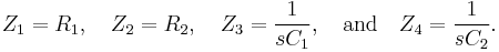
By choosing different passive components (e.g., resistors and capacitors) for , , , and , the filter can be made with low-pass, bandpass, and high-pass characteristics. In the examples below, recall that a resistor with resistance  has impedance
  of
of

and a capacitor with capacitance  has impedance
  of
of

where  and
and  is a frequency of a pure sine wave input. That is, a capacitor's impedance is frequency dependent and a resistor's impedance is not.
Example: Low-pass filter
An example of a unity-gain low-pass configuration is shown in Figure 2.
An operational amplifier is used as the buffer here, although an emitter follower is also effective. This circuit is equivalent to the generic case above with
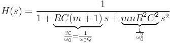
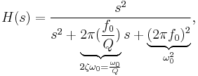
The transfer function for this second-order unity-gain low-pass filter is
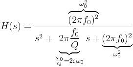
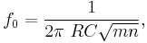
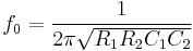
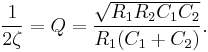
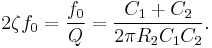
where the undamped natural frequency  and Q factor
  (i.e., damping ratio
  ) are given by
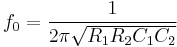
and
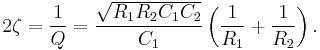
So,
The factor determines the height and width of the peak of the frequency response of the filter. As this parameter increases, the filter will tend to "ring" at a single resonant frequency near (see "LC filter" for a related discussion).
A designer must choose the and appropriate for his application. For example, a second-order Butterworth filter, which has maximally flat passband frequency response, has a of  . Because there are two parameters and four unknowns, the design procedure typically fixes one resistor as a ratio of the other resistor and one capacitor as a ratio of the other capacitor. One possibility is to set the ratio between
  and
and  as
as  and the ratio between
  and
and  as
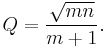
as  . So,
. So,


Therefore, the and expressions are
and
For example, the circuit in Figure 3 has an of  and a of
  . The transfer function is given by
and, after substitution, this expression is equal to
which shows how every  combination comes with some
  combination to provide the same
  and
and  for the low-pass filter. A similar design approach is used for the other filters below.
Example: High-pass filter
A second-order unity-gain high-pass filter with of  and of is shown in Figure 4.
A second-order unity-gain high-pass filter has the transfer function
where undamped natural frequency and factor are discussed above in the low-pass filter discussion. The circuit above implements this transfer function by the equations
(as before), and
So
Follow an approach similar to the one used to design the low-pass filter above.
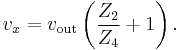
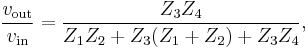
VCVS Example: Bandpass configuration
An example of a non-unity-gain bandpass filter implemented with a VCVS filter is shown in Figure 5. Although it uses a different topology and an operational amplifier configured to provide non-unity-gain, it can be analyzed using similar methods as with the generic Sallen–Key topology. Its transfer function is given by:
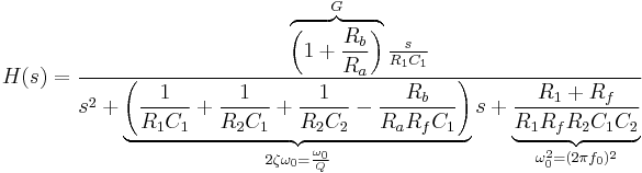
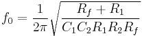
The center frequency (i.e., the frequency where the magnitude response has its peak) is given by:
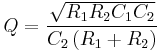
The Q factor is given by
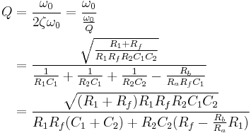
The voltage divider in the negative feedback loop controls the gain. The "inner gain"  provided by the operational amplifier is given by
while the amplifier gain at the peak frequency is given by:

It can be seen that must be kept below 3 or else the filter will oscillate. Practical component choices have  and
and  .
.
See also
External links
- Texas Instruments Application Report: Analysis of the Sallen–Key Architecture
- Analog Devices filter design applet – A simple online tool for designing active filters using voltage-feedback op-amps.
- TI active filter design source FAQ
- Op Amps for Everyone – Chapter 16
- High frequency modification of Sallen-Key filter - improving the stopband attenuation floor
- Online Calculation Tool for Sallen–Key Low-pass/High-pass Filters
- Online Calculation Tool for Filter Design and Analysis
- ECE 327: Procedures for Output Filtering Lab – Section 3 ("Smoothing Low-Pass Filter") discusses active filtering with Sallen–Key Butterworth low-pass filter.
References
- ^ a b "EE315A Course Notes - Chapter 2"-B. Murmann
- ^ Sallen, R. P.; E. L. Key (1955-03). "A Practical Method of Designing RC Active Filters". IRE Transactions on Circuit Theory 2 (1): 74–85.