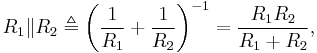
Operational amplifier applications
This article illustrates some typical applications of operational amplifiers. A simplified schematic notation is used, and the reader is reminded that many details such as device selection and power supply connections are not shown.
Contents |
Practical considerations
Input offset problems
It is important to note that the equations shown below, pertaining to each type of circuit, assume that an ideal op amp is used. Those interested in construction of any of these circuits for practical use should consult a more detailed reference. See the External links and Further reading sections.
Resistors used in practical solid-state op-amp circuits are typically in the kΩ range. Resistors much greater than 1 MΩ cause excessive thermal noise and make the circuit operation susceptible to significant errors due to bias or leakage currents.
Practical operational amplifiers draw a small current from each of their inputs due to bias requirements and leakage. These currents flow through the resistances connected to the inputs and produce small voltage drops across those resistances. In AC signal applications this seldom matters. If high-precision DC operation is required, however, these voltage drops need to be considered. The design technique is to try to ensure that these voltage drops are equal for both inputs, and therefore cancel. If these voltage drops are equal and the common-mode rejection ratio of the operational amplifier is good, there will be considerable cancellation and improvement in DC accuracy.
If the input currents into the operational amplifier are equal, to reduce offset voltage the designer must ensure that the DC resistance looking out of each input is also matched. In general input currents differ, the difference being called the input offset current, Ios. Matched external input resistances Rin will still produce an input voltage error of Rin·Ios . Most manufacturers provide a method for tuning the operational amplifier to balance the input currents (e.g., "offset null" or "balance" pins that can interact with an external voltage source attached to a potentiometer). Otherwise, a tunable external voltage can be added to one of the inputs in order to balance out the offset effect. In cases where a design calls for one input to be short-circuited to ground, that short circuit can be replaced with a variable resistance that can be tuned to mitigate the offset problem.
Note that many operational amplifiers that have MOSFET-based input stages have input leakage currents that will truly be negligible to most designs.
Power supply effects
Although the power supplies are not shown in the operational amplifier designs below, they can be critical in operational amplifier design.
Power supply imperfections (e.g., power signal ripple, non-zero source impedance) may lead to noticeable deviations from ideal operational amplifier behavior. For example, operational amplifiers have a specified power supply rejection ratio that indicates how well the output can reject signals that appear on the power supply inputs. Power supply inputs are often noisy in large designs because the power supply is used by nearly every component in the design, and inductance effects prevent current from being instantaneously delivered to every component at once. As a consequence, when a component requires large injections of current (e.g., a digital component that is frequently switching from one state to another), nearby components can experience sagging at their connection to the power supply. This problem can be mitigated with copious use of bypass capacitors connected across each power supply pin and ground. When bursts of current are required by a component, the component can bypass the power supply by receiving the current directly from the nearby capacitor (which is then slowly recharged by the power supply).
Additionally, current drawn into the operational amplifier from the power supply can be used as inputs to external circuitry that augment the capabilities of the operational amplifier. For example, an operational amplifier may not be fit for a particular high-gain application because its output would be required to generate signals outside of the safe range generated by the amplifier. In this case, an external push–pull amplifier can be controlled by the current into and out of the operational amplifier. Thus, the operational amplifier may itself operate within its factory specified bounds while still allowing the negative feedback path to include a large output signal well outside of those bounds.[1]
Amplifiers
Inverting amplifier
An inverting amplifier uses negative feedback[2] to invert (i.e., negate) and amplify a voltage. In particular, the Rin–Rf resistor network acts as an electronic seesaw (i.e., a class-1 lever) where the inverting (i.e., −) input of the operational amplifier is like a fulcrum about which the seesaw pivots. That is, because the operational amplifier is in a negative-feedback configuration, its internal high gain effectively fixes the inverting (i.e., −) input at the same 0 V (ground) voltage of the non-inverting (i.e., +) input, which is similar to the stiff mechanical support provided by the fulcrum of the seesaw. Continuing the analogy,
- Just as the movement of one end of the seesaw is opposite the movement of the other end of the seesaw, positive movement away from 0 V at the input of the Rin–Rf network is matched by negative movement away from 0 V at the output of the network; thus, the amplifier is said to be inverting.
- In the seesaw analogy, the mechanical moment or torque from the force on one side of the fulcrum is balanced exactly by the force on the other side of the fulcrum; consequently, asymmetric lengths in the seesaw allow for small forces on one side of the seesaw to generate large forces on the other side of the seesaw. In the inverting amplifier, electrical current, like torque, is conserved across the Rin–Rf network and relative differences between the Rin and Rf resistors allow small voltages on one side of the network to generate large voltages (with opposite sign) on the other side of the network. Thus, the device amplifies (and inverts) the input voltage. However, in this analogy, it is the reciprocals of the resistances (i.e., the conductances or admittances) that play the role of lengths in the seesaw.
Hence, the amplifier output is related to the input as in
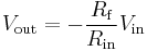 .
.
So the voltage gain of the amplifier is 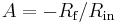 where the negative sign is a convention indicating that the output is negated. For example, if Rf is 10 kΩ and Rin is 1 kΩ, then the gain is −10 kΩ/1 kΩ, or −10 (or −10 V/V).[2] Moreover, the input impedance of the device is
  because the operational amplifier's inverting (i.e., −) input is a virtual ground.
In a real operational amplifier, the current into its two inputs is small but non-zero (e.g., due to input bias currents). The current into the inverting (i.e., −) input of the operational amplifier is drawn across the Rin and Rf resistors in parallel, which appears like a small parasitic voltage difference between the inverting (i.e., −) and non-inverting (i.e., +) inputs of the operational amplifier. To mitigate this practical problem, a third resistor of value 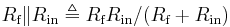 can be added between the non-inverting (i.e., +) input and the true ground.[3] This resistor does not affect the idealized operation of the device because no current enters the ideal non-inverting input. However, in the practical case, if input currents are roughly equivalent, the voltage added at the inverting input will match the voltage at the non-inverting input, and so this common-mode signal will be ignored by the operational amplifier (which operates on differences between its inputs).
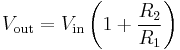
Non-inverting amplifier
Amplifies a voltage (multiplies by a constant greater than 1)
- Input impedance

- The input impedance is at least the impedance between non-inverting (
 ) and inverting (
 ) inputs, which is typically 1 MΩ to 10 TΩ, plus the impedance of the path from the inverting () input to ground (i.e.,
  in parallel with
  ).
). - Because negative feedback ensures that the non-inverting and inverting inputs match, the input impedance is actually much higher.
- The input impedance is at least the impedance between non-inverting (
- Although this circuit has a large input impedance, it suffers from error of input bias current.
- The non-inverting () and inverting () inputs draw small leakage currents into the operational amplifier.
- These input currents generate voltages that act like unmodeled input offsets. These unmodeled effects can lead to noise on the output (e.g., offsets or drift).
- Assuming that the two leaking currents are matched, their effect can be mitigated by ensuring the DC impedance looking out of each input is the same.
- The voltage produced by each bias current is equal to the product of the bias current with the equivalent DC impedance looking out of each input. Making those impedances equal makes the offset voltage at each input equal, and so the non-zero bias currents will have no impact on the difference between the two inputs.
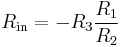
- A resistor of value
- which is the equivalent resistance of in parallel with , between the
 source and the non-inverting () input will ensure the impedances looking out of each input will be matched.
- The matched bias currents will then generate matched offset voltages, and their effect will be hidden to the operational amplifier (which acts on the difference between its inputs) so long as the CMRR is good.
- Very often, the input currents are not matched.
- Most operational amplifiers provide some method of balancing the two input currents (e.g., by way of an external potentiometer).
- Alternatively, an external offset can be added to the operational amplifier input to nullify the effect.
- Another solution is to insert a variable resistor between the source and the non-inverting () input. The resistance can be tuned until the offset voltages at each input are matched.
- Operational amplifiers with MOSFET-based input stages have input currents that are so small that they often can be neglected.
- The non-inverting (
Differential amplifier
- The name "differential amplifier" should not be confused with the "differentiator," which is also shown on this page.
- The "instrumentation amplifier," which is also shown on this page, is a modification of the differential amplifier that also provides high input impedance.
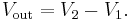
The circuit shown computes the difference of two voltages multiplied by some constant. In particular, the output voltage is:
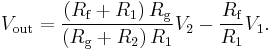
The differential input impedance Zin (i.e., the impedance between the two input pins) is approximately R1 + R2. The input currents vary with the operating point of the circuit. Consequently, if the two sources feeding this circuit have appreciable output impedance, then non-linearities can appear in the output. An instrumentation amplifier mitigates these problems.
- Under the condition that the Rf/R1 = Rg/R2, the output expression becomes:
-
 where
where  is the differential gain of the circuit.
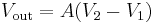
- Moreover, the amplifier synthesized with this choice of parameters has good common-mode rejection in theory because components of the signals that have V1 = V2 are not expressed on the output. Although this property is described here with resistances, it is a more general property of the impedances in the circuit. So, for example, if a compensation capacitor is added across any resistor (e.g., to improve phase margin and ensure closed-loop stability of the operational amplifier), similar changes need to be made in the rest of the circuit to maintain the ratio balance. Otherwise, high-frequency components common to both V1 and V2 can express themselves on the output. Additionally, because of leakage or bias currents in a real operational amplifier, it is usually desirable for the impedance looking out each input to the operational amplifier to be equal to the impedance looking out of the other input of the operational amplifier. Otherwise, the same current into each operational amplifier input will generate a parasitic differential signal and thus a parasitic output component. Consequently, choosing R1 = R2 and Rf = Rg is common in practice.
- In the special case when Rf/R1 = Rg/R2, as before, and Rf = R1, the differential gain A = 1, and the circuit is a differential follower with:
Voltage follower (Unity Buffer Amplifier)
Used as a buffer amplifier to eliminate loading effects (e.g., connecting a device with a high source impedance to a device with a low input impedance).

 (realistically, the differential input impedance of the op-amp itself, 1 MΩ to 1 TΩ)
Due to the strong (i.e., unity gain) feedback and certain non-ideal characteristics of real operational amplifiers, this feedback system is prone to have poor stability margins. Consequently, the system may be unstable when connected to sufficiently capacitive loads. In these cases, a lag compensation network (e.g., connecting the load to the voltage follower through a resistor) can be used to restore stability. The manufacturer data sheet for the operational amplifier may provide guidance for the selection of components in external compensation networks. Alternatively, another operational amplifier can be chosen that has more appropriate internal compensation.
Summing amplifier
A summing amplifier sums several (weighted) voltages:
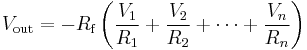
- When
 , and
, and  independent
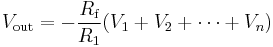
- When


- Output is inverted
- Input impedance of the nth input is
 (
( is a virtual ground)
Instrumentation amplifier
Combines very high input impedance, high common-mode rejection, low DC offset, and other properties used in making very accurate, low-noise measurements
- Is made by adding a non-inverting buffer to each input of the differential amplifier to increase the input impedance.
Oscillators
Wien bridge oscillator
Produces a very low distortion sine wave. Uses negative temperature compensation in the form of a light bulb or diode.
Relaxation oscillator
By using an RC network to add slow negative feedback to the inverting Schmitt trigger, a relaxation oscillator is formed. The feedback through the RC network causes the Schmitt trigger output to oscillate in an endless symmetric square wave (i.e., the Schmitt trigger in this configuration is an astable multivibrator).
Filters
Operational amplifiers can be used in construction of active filters, providing high-pass, low-pass, band-pass, reject and delay functions. The high input impedance and gain of an op-amp allow straightforward calculation of element values, allowing accurate implementation of any desired filter topology with little concern for the loading effects of stages in the filter or of subsequent stages. However, the frequencies at which active filters can be implemented is limited; when the behavior of the amplifiers departs significantly from the ideal behavior assumed in elementary design of the filters, filter performance is degraded.
Comparators and detectors
Comparator
Bistable output that indicates which of the two inputs has a higher voltage. That is,
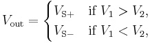
where  and
and  are nominally the positive and negative supply voltages (which are not shown in the diagram).
Threshold detector
The threshold detector with hysteresis, very similar to the zero crossing threshold detector, consists of an operational amplifier and a series of resistors that provide hysteresis. Like other detectors, this device functions as a voltage switch, but with an important difference. The state of the detector output is not directly affected by input voltage, but instead by the voltage drop across its input terminals (here, referred to as Va). From Kirchhoff's Current Law, this value depends both on Vin and the output voltage of the threshold detector itself, both multiplied by a resistor ratio.
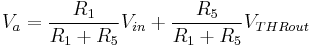
Unlike the zero crossing detector, the detector with hysteresis does not switch when Vin is zero, rather the output becomes Vsat+ when Va becomes positive and Vsat- when Va becomes negative. Further examination of the Va equation reveals that Vin can exceed zero (positive or negative) by a certain magnitude before the output of the detector is caused to switch. By adjusting the value of R1, the magnitude of Vin that will cause the detector to switch can be increased or decreased. This property often proves very useful in various applications, including signal generators.
Zero level detector
A zero crossing detector is a comparator with the reference level set at zero. It is used for detecting the zero crossings of AC signals. It can be made from an operational amplifier with an input voltage at its positive input (see circuit diagram).
When the input voltage is positive, the output voltage is a positive value, when the input voltage is negative, the output voltage is a negative value. The magnitude of the output voltage is a property of the operational amplifier and its power supply. When used with a ±15 V power supply and a 741C operational amplifier, Vsat+ is approximately 13.6 V and Vsat- is approximately -14.3 V.
Schmitt trigger
A bistable multivibrator implemented as a comparator with hysteresis.
In this configuration, the input voltage is applied through the resistor  (which may be the source internal resistance) to the non-inverting input and the inverting input is grounded or referenced. The hysteresis curve is non-inverting and the switching thresholds are
  where
where  is the greatest output magnitude of the operational amplifier.
Alternatively, the input source and the ground may be swapped. Now the input voltage is applied directly to the inverting input and the non-inverting input is grounded or referenced. The hysteresis curve is inverting and the switching thresholds are 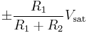 . Such a configuration is used in the relaxation oscillator shown below.
Integration and differentiation
Inverting integrator
Integrates the (inverted) signal over time
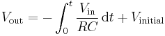
(where and  are functions of time,
  is the output voltage of the integrator at time t = 0.)
- Note that this can also be viewed as a low-pass electronic filter. It is a filter with a single pole at DC (i.e., where
 ) and gain.
 - There are several potential problems with this circuit.
- It is usually assumed that the input has zero DC component (i.e., has a zero average value). Otherwise, unless the capacitor is periodically discharged, the output will drift outside of the operational amplifier's operating range.
- Even when has no offset, the leakage or bias currents into the operational amplifier inputs can add an unexpected offset voltage to that causes the output to drift. Balancing input currents and replacing the non-inverting () short-circuit to ground with a resistor with resistance
 can reduce the severity of this problem.
 - Because this circuit provides no DC feedback (i.e., the capacitor appears like an open circuit to signals with ), the offset of the output may not agree with expectations (i.e., may be out of the designer's control with the present circuit).
- It is usually assumed that the input
- Many of these problems can be made less severe by adding a large resistor
 in parallel with the feedback capacitor. At significantly high frequencies, this resistor will have negligible effect. However, at low frequencies where there are drift and offset problems, the resistor provides the necessary feedback to hold the output steady at the correct value. In effect, this resistor reduces the DC gain of the "integrator" – it goes from infinite to some finite value
  .
.
Inverting differentiator
Differentiates the (inverted) signal over time.

- Note that this can also be viewed as a high-pass electronic filter. It is a filter with a single zero at DC (i.e., where angular frequency radians) and gain. The high-pass characteristics of a differentiating amplifier (i.e., the low-frequency zero) can lead to stability challenges when the circuit is used in an analog servo loop (e.g., in a PID controller with a significant derivative gain). In particular, as a root locus analysis would show, increasing feedback gain will drive a closed-loop pole toward marginal stability at the DC zero introduced by the differentiator.
Synthetic elements
Inductance gyrator
Simulates an inductor (i.e., provides inductance without the use of a possibly costly inductor). The circuit exploits the fact that the current flowing through a capacitor behaves through time as the voltage across an inductor. The capacitor used in this circuit is smaller than the inductor it simulates and its capacitance is less subject to changes in value due to environmental changes.
This circuit is unsuitable for applications relying on the back EMF property of an inductor as this will be limited in a gyrator circuit to the voltage supplies of the op-amp.
Negative impedance converter (NIC)
Creates a resistor having a negative value for any signal generator
- In this case, the ratio between the input voltage and the input current (thus the input resistance) is given by:
In general, the components , , and  need not be resistors; they can be any component that can be described with an impedance.
Non-linear
Precision rectifier
The voltage drop VF across the forward biased diode in the circuit of a passive rectifier is undesired. In this active version, the problem is solved by connecting the diode in the negative feedback loop. The op-amp compares the output voltage across the load with the input voltage and increases its own output voltage with the value of VF. As a result, the voltage drop VF is compensated and the circuit behaves very nearly as an ideal (super) diode with VF = 0 V.
The circuit has speed limitations at high frequency because of the slow negative feedback and due to the low slew rate of many non-ideal op-amps.
Logarithmic output
- The relationship between the input voltage
 and the output voltage
  is given by:
- where
 is the saturation current and
  is the thermal voltage.
- If the operational amplifier is considered ideal, the negative pin is virtually grounded, so the current flowing into the resistor from the source (and thus through the diode to the output, since the op-amp inputs draw no current) is:
- where
 is the current through the diode. As known, the relationship between the current and the voltage for a diode is:
- This, when the voltage is greater than zero, can be approximated by:
- Putting these two formulae together and considering that the output voltage is the negative of the voltage across the diode (
 ), the relationship is proven.
Note that this implementation does not consider temperature stability and other non-ideal effects.
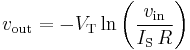
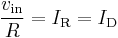
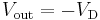
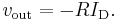
Exponential output
- The relationship between the input voltage and the output voltage is given by:
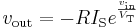
where is the saturation current and is the thermal voltage.
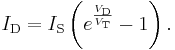
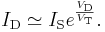
- Considering the operational amplifier ideal, then the negative pin is virtually grounded, so the current through the diode is given by:
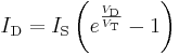
when the voltage is greater than zero, it can be approximated by:
The output voltage is given by:
Other applications
See also
- Current-feedback operational amplifier
- Frequency compensation
- Operational amplifier
- Operational transconductance amplifier
- Miller theorem applications closely related to the op-amp circuits from this article
References
- ^ Paul Horowitz and Winfield Hill, The Art of Electronics. 2nd ed. Cambridge University Press, Cambridge, 1989 ISBN 0-521-37095-7
- ^ a b Basic Electronics Theory, Delton T. Horn, 4th ed. McGraw-Hill Professional, 1994, p. 342–343.
- ^ Malmstadt, Enke and Crouch, Electronics and Instrumentation for Scientists, The Benjamin/Cummings Publishing Company, Inc., 1981, ISBN 0-8053-6917-1, Chapter 5. p. 118.
Further reading
- Paul Horowitz and Winfield Hill, The Art of Electronics. 2nd ed. Cambridge University Press, Cambridge, 1989 ISBN 0-521-37095-7
- Sergio Franco, Design with Operational Amplifiers and Analog Integrated Circuits, 3rd ed., McGraw-Hill, New York, 2002 ISBN 0-07-232084-2
External links
- Op Amps for EveryonePDF (1.96 MiB)
- Single supply op-amp circuit collectionPDF (163 KiB)
- Op-amp circuit collectionPDF (962 KiB)
- A Collection of Amp ApplicationsPDF (1.06 MiB) – Analog Devices Application note
- Basic OpAmp ApplicationsPDF (173 KiB)
- Handbook of operational amplifier applicationsPDF (2.00 MiB) – Texas Instruments Application note
- Low Side Current Sensing Using Operational Amplifiers
- Log/anti-log generators, cube generator, multiply/divide ampPDF (165 KiB)
- Logarithmically variable gain from a linear variable component
- Impedance and admittance transformations using operational amplifiers by D. H. Sheingold