Electron microscope
An electron microscope is a type of microscope that uses electrons to illuminate a specimen and create an enlarged image. Electron microscopes have much greater resolving power than light microscopes and can obtain much higher magnifications. Some electron microscopes can magnify specimens up to 2 million times, while the best light microscopes are limited to magnifications of 2000 times. Both electron and light microscopes have resolution limitations, imposed by their wavelength. The greater resolution and magnification of the electron microscope is due to the wavelength of an electron, its de Broglie wavelength, being much smaller than that of a light photon, electromagnetic radiation.
The electron microscope uses electrostatic and electromagnetic lenses in forming the image by controlling the electron beam to focus it at a specific plane relative to the specimen in a manner similar to how a light microscope uses glass lenses to focus light on or through a specimen to form an image.
Contents |
History
The first electron microscope prototype was built in 1931 by the German engineers Ernst Ruska and Max Knoll.[1] Although this initial instrument was capable of magnifying objects by only four hundred times, it demonstrated the principles of an electron microscope. Two years later, Ruska constructed an electron microscope that exceeded the resolution possible with an optical microscope.[1]
Reinhold Rudenberg, the research director of Siemens, had patented the electron microscope in 1931, although Siemens was doing no research on electron microscopes at that time. In 1937 Siemens began funding Ruska and Bodo von Borries to develop an electron microscope. Siemens also employed Ruska's brother Helmut to work on applications, particularly with biological specimens.[2][3]
In the same decade Manfred von Ardenne pioneered the scanning electron microscope and his universal electron microscope.[4]
Siemens produced the first commercial TEM in 1939, but the first practical electron microscope had been built at the University of Toronto in 1938, by Eli Franklin Burton and students Cecil Hall, James Hillier, and Albert Prebus.[5]
Although modern electron microscopes can magnify objects up to two million times, they are still based upon Ruska's prototype. The electron microscope is an essential item of equipment in many laboratories. Researchers use them to examine biological materials (such as microorganisms and cells), a variety of large molecules, medical biopsy samples, metals and crystalline structures and the characteristics of various surfaces. The electron microscope is also used extensively for inspection, quality assurance and failure analysis applications in industry, including, in particular, semiconductor device fabrication.
Types
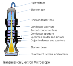
Transmission Electron Microscope (TEM)
The original form of electron microscope, the transmission electron microscope (TEM) uses a high voltage electron beam to create an image. The electrons are emitted by an electron gun, commonly fitted with a tungsten filament cathode as the electron source. The electron beam is accelerated by an anode typically at +100keV (40 to 400 keV) with respect to the cathode, focused by electrostatic and electromagnetic lenses, and transmitted through the specimen that is in part transparent to electrons and in part scatters them out of the beam. When it emerges from the specimen, the electron beam carries information about the structure of the specimen that is magnified by the objective lens system of the microscope. The spatial variation in this information (the "image") is viewed by projecting the magnified electron image onto a fluorescent viewing screen coated with a phosphor or scintillator material such as zinc sulfide. The image can be photographically recorded by exposing a photographic film or plate directly to the electron beam, or a high-resolution phosphor may be coupled by means of a lens optical system or a fibre optic light-guide to the sensor of a CCD (charge-coupled device) camera. The image detected by the CCD may be displayed on a monitor or computer.
Resolution of the TEM is limited primarily by spherical aberration, but a new generation of aberration correctors have been able to partially overcome spherical aberration to increase resolution. Software correction of spherical aberration for the High Resolution TEM HRTEM has allowed the production of images with sufficient resolution to show carbon atoms in diamond separated by only 0.89 ångström (89 picometers) and atoms in silicon at 0.78 ångström (78 picometers)[6][7] at magnifications of 50 million times.[8] The ability to determine the positions of atoms within materials has made the HRTEM an important tool for nano-technologies research and development.
Scanning Electron Microscope (SEM)
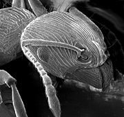
Unlike the TEM, where electrons of the high voltage beam carry the image of the specimen, the electron beam of the Scanning Electron Microscope (SEM)[9] does not at any time carry a complete image of the specimen. The SEM produces images by probing the specimen with a focussed electron beam that is scanned across a rectangular area of the specimen. At each point on the specimen the incident electron beam loses some energy, and that lost energy is converted into other forms, such as heat, emission of low-energy secondary electrons, light emission (cathodoluminescence) or x-ray emission. The display of the SEM maps the varying intensity of any of these signals into the image in a position corresponding to the position of the beam on the specimen when the signal was generated. In the SEM image of an ant shown at right, the image was constructed from signals produced by a secondary electron detector, the normal or conventional imaging mode in most SEMs.
Generally, the image resolution of an SEM is about an order of magnitude poorer than that of a TEM. However, because the SEM image relies on surface processes rather than transmission it is able to image bulk samples up to several centimetres in size (depending on instrument design) and has a much greater depth of view, and so can produce images that are a good representation of the 3D structure of the sample.
Reflection Electron Microscope (REM)
In the Reflection Electron Microscope (REM) as in the TEM, an electron beam is incident on a surface, but instead of using the transmission (TEM) or secondary electrons (SEM), the reflected beam of elastically scattered electrons is detected. This technique is typically coupled with Reflection High Energy Electron Diffraction and Reflection high-energy loss spectrum (RHELS). Another variation is Spin-Polarized Low-Energy Electron Microscopy (SPLEEM), which is used for looking at the microstructure of magnetic domains.[10]
Scanning Transmission Electron Microscope (STEM)
The STEM rasters a focused incident probe across a specimen that (as with the TEM) has been thinned to facilitate detection of electrons scattered through the specimen. The high resolution of the TEM is thus possible in STEM. The focusing action (and aberrations) occur before the electrons hit the specimen in the STEM, but afterward in the TEM. The STEM's use of SEM-like beam rastering simplifies annular dark-field imaging, and other analytical techniques, but also means that image data is acquired in serial rather than in parallel fashion.
Sample preparation

Materials to be viewed under an electron microscope may require processing to produce a suitable sample. The technique required varies depending on the specimen and the analysis required:
- Chemical Fixation for biological specimens aims to stabilize the specimen's mobile macromolecular structure by chemical crosslinking of proteins with aldehydes such as formaldehyde and glutaraldehyde, and lipids with osmium tetroxide.
- Cryofixation – freezing a specimen so rapidly, to liquid nitrogen or even liquid helium temperatures, that the water forms vitreous (non-crystalline) ice. This preserves the specimen in a snapshot of its solution state. An entire field called cryo-electron microscopy has branched from this technique. With the development of cryo-electron microscopy of vitreous sections (CEMOVIS), it is now possible to observe virtually any biological specimen close to its native state.
- Dehydration – freeze drying, or replacement of water with organic solvents such as ethanol or acetone, followed by critical point drying or infiltration with embedding resins.
- Embedding, biological specimens – after dehydration, tissue for observation in the transmission electron microscope is embedded so it can be sectioned ready for viewing. To do this the tissue is passed through a 'transition solvent' such as epoxy propane and then infiltrated with a resin such as Araldite epoxy resin; tissues may also be embedded directly in water-miscible acrylic resin. After the resin has been polymerised (hardened) the sample is thin sectioned (ultrathin sections) and stained - it is then ready for viewing.
- Embedding, materials - after embedding in resin, the specimen is usually ground and polished to a mirror-like finish using ultra-fine abrasives. The polishing process must be performed carefully to minimise scratches and other polishing artefacts that reduce image quality.
- Sectioning – produces thin slices of specimen, semitransparent to electrons. These can be cut on an ultramicrotome with a diamond knife to produce ultrathin slices about 60-90nm thick. Disposable glass knives are also used because they can be made in the lab and are much cheaper.
- Staining – uses heavy metals such as lead, uranium or tungsten to scatter imaging electrons and thus give contrast between different structures, since many (especially biological) materials are nearly "transparent" to electrons (weak phase objects). In biology, specimens are can be stained "en bloc" before embedding and also later after sectioning. Typically thin sections are stained for several minutes with an aqueous or acoholic solution of uranyl acetate followed by aqueous lead citrate.
- Freeze-fracture or freeze-etch – a preparation method particularly useful for examining lipid membranes and their incorporated proteins in "face on" view. The fresh tissue or cell suspension is frozen rapidly (cryofixed), then fractured by simply breaking or by using a microtome while maintained at liquid nitrogen temperature. The cold fractured surface (sometimes "etched" by increasing the temperature to about -100°C for several minutes to let some ice sublime) is then shadowed with evaporated platinum or gold at an average angle of 45° in a high vacuum evaporator. A second coat of carbon, evaporated perpendicular to the average surface plane is often performed to improve stability of the replica coating. The specimen is returned to room temperature and pressure, then the extremely fragile "pre-shadowed" metal replica of the fracture surface is released from the underlying biological material by careful chemical digestion with acids, hypochlorite solution or SDS detergent. The still-floating replica is thoroughly washed from residual chemicals, carefully fished up on EM grids, dried then viewed in the TEM.
- Ion Beam Milling – thins samples until they are transparent to electrons by firing ions (typically argon) at the surface from an angle and sputtering material from the surface. A subclass of this is Focused ion beam milling, where gallium ions are used to produce an electron transparent membrane in a specific region of the sample, for example through a device within a microprocessor. Ion beam milling may also be used for cross-section polishing prior to SEM analysis of materials that are difficult to prepare using mechanical polishing.
- Conductive Coating – An ultrathin coating of electrically-conducting material, deposited either by high vacuum evaporation or by low vacuum sputter coating of the sample. This is done to prevent the accumulation of static electric fields at the specimen due to the electron irradiation required during imaging. Such coatings include gold, gold/palladium, platinum, tungsten, graphite etc. and are especially important for the study of specimens with the scanning electron microscope. Another reason for coating, even when there is more than enough conductivity, is to improve contrast, a situation more common with the operation of a FESEM (field emission SEM). When an osmium coater is used, a layer far thinner than would be possible with any of the previously mentioned sputtered coatings is possible.[11]
Disadvantages

Electron microscopes are expensive to build and maintain, but the capital and running costs of confocal light microscope systems now overlaps with those of basic electron microscopes. They are dynamic rather than static in their operation, requiring extremely stable high-voltage supplies, extremely stable currents to each electromagnetic coil/lens, continuously-pumped high- or ultra-high-vacuum systems, and a cooling water supply circulation through the lenses and pumps. As they are very sensitive to vibration and external magnetic fields, microscopes designed to achieve high resolutions must be housed in stable buildings (sometimes underground) with special services such as magnetic field cancelling systems. Some desktop low voltage electron microscopes have TEM capabilities at very low voltages (around 5 kV) without stringent voltage supply, lens coil current, cooling water or vibration isolation requirements and as such are much less expensive to buy and far easier to install and maintain, but do not have the same ultra-high (atomic scale) resolution capabilities as the larger instruments.
The samples largely have to be viewed in vacuum, as the molecules that make up air would scatter the electrons. One exception is the environmental scanning electron microscope, which allows hydrated samples to be viewed in a low-pressure (up to 20 Torr/2.7 kPa), wet environment.
Scanning electron microscopes usually image conductive or semi-conductive materials best. Non-conductive materials can be imaged by an environmental scanning electron microscope. A common preparation technique is to coat the sample with a several-nanometer layer of conductive material, such as gold, from a sputtering machine; however, this process has the potential to disturb delicate samples.
Small, stable specimens such as carbon nanotubes, diatom frustules and small mineral crystals (asbestos fibres, for example) require no special treatment before being examined in the electron microscope. Samples of hydrated materials, including almost all biological specimens have to be prepared in various ways to stabilize them, reduce their thickness (ultrathin sectioning) and increase their electron optical contrast (staining). There is a risk that these processes may result in artifacts, but these can usually be identified by comparing the results obtained by using radically different specimen preparation methods. It is generally believed by scientists working in the field that as results from various preparation techniques have been compared and that there is no reason that they should all produce similar artifacts, it is reasonable to believe that electron microscopy features correspond with those of living cells. In addition, higher-resolution work has been directly compared to results from X-ray crystallography, providing independent confirmation of the validity of this technique. Since the 1980s, analysis of cryofixed, vitrified specimens has also become increasingly used by scientists, further confirming the validity of this technique.[12][13][14]
Applications
-
Semiconductor and data storage
- Circuit edit
- Defect analysis
- Failure analysis
Biology and life sciences
- Diagnostic electron microscopy
- Cryobiology
- Protein localization
- Electron tomography
- Cellular tomography
- Cryo-electron microscopy
- Toxicology
- Biological production and viral load monitoring
- Particle analysis
- Pharmaceutical QC
- Structural biology
- 3D tissue imaging
- Virology
- Vitrification
Research
- Electron beam induced depostion
- Materials qualification
- Materials and sample preparation
- Nanoprototyping
- Nanometrology
- Device testing and characterization
Industry
- High-resolution imaging
- 2D & 3D micro-characterization
- Macro sample to nanometer metrology
- Particle detection and characterization
- Direct beam-writing fabrication
- Dynamic materials experiments
- Sample preparation
- Forensics
- Mining (mineral liberation analysis)
- Chemical/Petrochemical
See also
- Category:Electron microscope images
- Field emission microscope
- Scanning tunneling microscope
References
- ↑ 1.0 1.1 Ernst Ruska Nobel Prize autobiography
- ↑ Ernst Ruska (1986). "Ernst Ruska Autobiography". Nobel Foundation. Retrieved on 2007-02-06.
- ↑ DH Kruger, P Schneck and HR Gelderblom (May 13, 2000). "Helmut Ruska and the visualisation of viruses". The Lancet 355 (9216): 1713–1717. doi:.
- ↑ M von Ardenne and D Beischer (1940). "Untersuchung von metalloxud-rauchen mit dem universal-elektronenmikroskop" (in German). Zeitschrift Electrochemie 46: 270–277.
- ↑ MIT biography of Hillier
- ↑ OÅM: World-Record Resolution at 0.78 Å, (May 18, 2001) Berkeley Lab Currents.
- ↑ P. D. Nellist, M. F. Chisholm, N. Dellby, O. L. Krivanek, M. F. Murfitt, Z. S. Szilagyi, A. R. Lupini, A. Borisevich, W. H. Sides, Jr., S. J. Pennycook (September 17, 2004). "Direct Sub-Angstrom Imaging of a Crystal Lattice". Science 305 (5691): 1741. doi:. PMID 15375260. http://www.sciencemag.org/cgi/content/abstract/305/5691/1741.
- ↑ The Scale of Things, DOE Office of Basic Energy Sciences (BES).
- ↑ SCANNING ELECTRON MICROSCOPY 1928 - 1965
- ↑ NCEM National Center for Electron Microscopy: SPLEEM
- ↑ http://www.2spi.com/catalog/osmi-coat.html
- ↑ Adrian, Marc; Dubochet, Jacques; Lepault, Jean; McDowall, Alasdair W. (1984). "Cryo-electron microscopy of viruses". Nature 308 (5954): 32–36. doi:.
- ↑ Sabanay, I.; Arad, T.; Weiner, S.; Geiger, B. (1991). "Study of vitrified, unstained frozen tissue sections by cryoimmunoelectron microscopy". Journal of Cell Science 100 (1): 227–236. PMID 1795028. http://jcs.biologists.org/cgi/content/abstract/100/1/227.
- ↑ Kasas, S.; Dumas, G.; Dietler, G.; Catsicas, S.; Adrian, M. (2003). "Vitrification of cryoelectron microscopy specimens revealed by high-speed photographic imaging". Journal of Microscopy 211 (1): 48–53. doi:.
External links
General
- electron microscopy Website of the ETH Zurich: Very good graphics and images, which illustrate various procedures.
- Environmental Scanning Electron Microscope (ESEM)
- X-ray element analysis in electron microscope – Information portal with X-ray microanalysis and EDX contents
History
- John H.L. Watson: Very early Electron Microscopy in the Department of Physics, the University of Toronto – A personal recollection
- Rubin Borasky Electron Microscopy Collection, 1930-1988 Archives Center, National Museum of American History, Smithsonian Institution.